
Mist fabrication of quantum dot devices

a fabrication process and quantum dot technology, applied in the direction of nanoinformatics, liquid/solution decomposition chemical coating, discharge tube luminescnet screen, etc., to achieve the effect of efficient deposition and patterning of qd layers

Inactive Publication Date: 2008-10-02
PENN STATE RES FOUND
View PDF23 Cites 91 Cited by
  • Summary
  • Abstract
  • Description
  • Claims
  • Application Information

AI Technical Summary

Benefits of technology

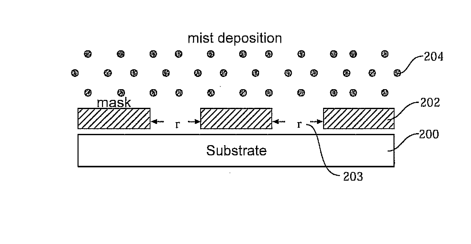
[0011]The use of shadow masks allows spatial patterning of a deposited film. Efficient deposition and patterning of QD layers, for displays and other applications, can be achieved using selective area mist deposition using a shadow mask. Precise controls over thickness (for example, within + / − one quantum dot diameter), composition (for example, substantially compositionally uniform emissive materials within a desired area of the substrate), surface morphology, and display resolution (for display applications) can be achieved. Multi-color QD-LEDs can be fabricated over large surface areas for passive or active matrix display applications.
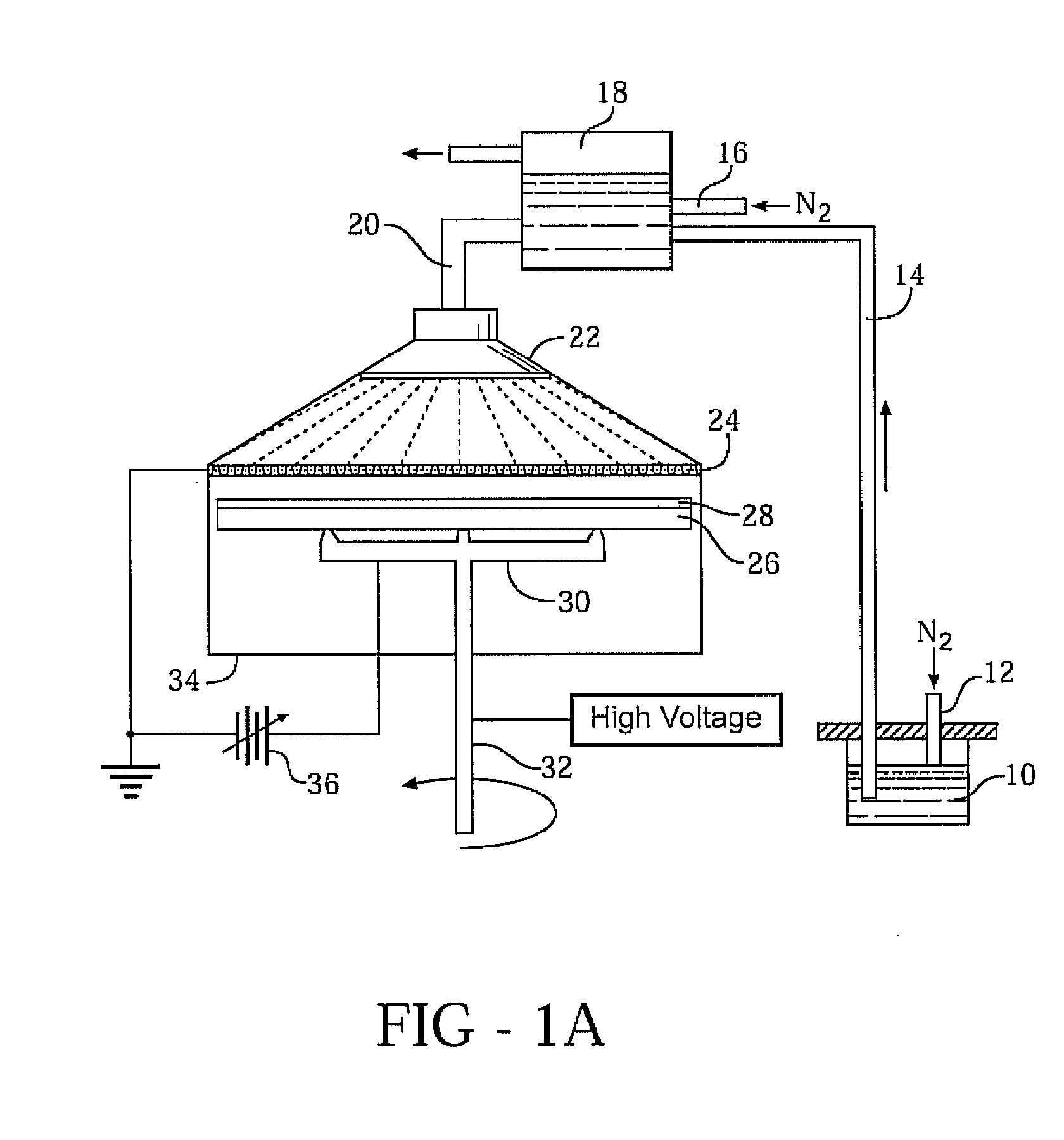
[0013]The temperature of the substrate may be near room temperature, e.g. 20-25° C. The precursor liquid film on the substrate can be patterned using a shadow mask, and a thermal treatment (and / or other processes) can be used to remove some or all of the liquid carrier, giving a solid film. The deposition rate can be controlled by imparting an electrical charge to the droplets, and accelerating the droplets towards the substrate using an electric field, Deposition and patterning of films can be facilitated using choice of liquid carrier (e.g. polar or non-polar liquid carriers), substrate surface energy (e.g. hydrophilic or hydrophobic), and also surface features (e.g. ridges that facilitate film flow along but not across the ridges).

Problems solved by technology

There are great challenges to address along the roadmap of QD-LED display technology.

Method used


Image

  • Mist fabrication of quantum dot devices
  • Mist fabrication of quantum dot devices
  • Mist fabrication of quantum dot devices

Examples


example display fabrication

[0066]RGB-pixel arrays of bright QD-LEDs were designed and fabricated using the selective area mist deposition of multi-color QDs.

[0067]FIG. 5A illustrates generally a 6×6 matrix of alternating pixels comprising 5 nm-diameter CdSe / ZnS QDs (green) and 8 nm-diameter CdSe / ZnS QDs (red) on a glass substrate fabricated by sequential mist-deposited though two optically-aligned shadow masks. The emission wavelength is tuned using the QD diameter.

[0068]FIG. 5C shows a fluorescence image taken under UV-illumination. The surface dimension of each QD pixel, such as pixel 132, is 500 μm×500 μm. The thickness of the pixelated film is ˜50 nm for red QDs (6 ML) and ˜30 nm for green QDs (6 ML), which were chosen to ease the observation of fluorescence images.

[0069]The photoluminescence spectra of the patterned QD pixels, as illustrated in FIG. 5B, are identical to that of the QD solutions used for mist deposition. Successful patterning of QD-emitter arrays was accomplished for pixels of varying siz...


PUM

PropertyMeasurementUnit
Lengthaaaaaaaaaa
Lengthaaaaaaaaaa
Lengthaaaaaaaaaa

Abstract

An example quantum dot (QD) device comprises a QD layer on a substrate, and may be fabricated by aerosol deposition, for example by mist deposition. An example approach includes providing a liquid precursor including QDs dispersed in a liquid carrier, generating a mist of droplets of the liquid precursor, directing the droplets towards the substrate so as to form a liquid precursor film on the substrate, and removing the liquid carrier from the liquid precursor film to form the quantum dot layer on the substrate. Example devices include multi-color QD-LED (light emitting diode) displays, and other devices.

Description

REFERENCE TO RELATED APPLICATIONS[0001]This application claims priority from U.S. Provisional Patent Application Ser. Nos. 60 / 909,160, filed Mar. 30, 2007 and 60 / 975,270, filed Sep. 26, 2007, the entire content of both of which are incorporated herein by reference.FIELD OF THE INVENTION[0002]The present invention relates to improved deposition processes for device fabrication, and to devices fabricated using such processes, for example electronic displays such as quantum dot light emitting diodes (QD-LEDs).BACKGROUND OF THE INVENTION[0003]Semiconductor quantum dots (QDs) have recently commanded considerable attention from photonics researchers due to their interesting optical characteristics. Semiconductor QDs are typically nanocrystals (nanocrystal quantum dots, NQDs) that are smaller in size than the diameter of a Bohr exciton in a bulk crystal of the same material. The small dimensions of QDs can, therefore, apply extremely strong quantum confinement to their electronic structure...

Claims


Application Information

Patent Timeline
IPC IPC(8): H01J1/62B05D1/06
CPCB22F9/026B82Y10/00B82Y15/00B82Y20/00B82Y30/00C23C18/1258C23C18/127C23C18/1295H01L31/035281H01L31/04Y10S438/962
Inventor XU, JIANRUZYLLO, JERZYSHANMUGASUNDARAM, KARTHIKEYANZHU, TINGZHANG, FAN
Owner PENN STATE RES FOUND
Learn More