
Method for Fabricating a P-I-N Light Emitting Diode Using Cu-Doped P-Type Zno

a light-emitting diode and pin-type technology, applied in the direction of basic electric elements, electrical apparatus, semiconductor devices, etc., can solve the problems of low solubility of p-type dopant, difficult preparation of high-concentration p-type dopant, and inability to achieve stable p-type thin film for a basic pn junction structure required for application of leds or laser diodes. , to achieve the effect of fast response time and high efficiency

Inactive Publication Date: 2008-09-25
KOREA INST OF SCI & TECH
View PDF6 Cites 10 Cited by
  • Summary
  • Abstract
  • Description
  • Claims
  • Application Information

AI Technical Summary

Benefits of technology

[0010]The present invention provides a method of fabricating a p-i-n type LED using p-type ZnO. Conventionally, a p-type ZnO thin film was difficult to reproducibly manufacture, attributed to the low solubility at high temperatures and the formation of various intermediate phases at relatively low temperatures of the Group 5 element, including N, P, As or Sb, known as a typical p-type ZnO dopant. However, according to the method of the present invention, a p-type ZnO thin film can be manufactured through post-heat treatment in an oxygen atmosphere under relatively high pressure using a copper dopant. In this way, the stable p-type ZnO thin film can be manufactured, and thus, it is possible to fabricate novel LEDs and laser diodes having high efficiencies in the near UV and visible regions. As well, electrical devices operated at high temperatures can be fabricated.
[0011]In addition, through the fabrication of pin or pn UV detectors having fast response times, fire alarms and underwater communication and visible blind detectors can be manufactured.
[0012]In addition, it is possible to manufacture a transparent thin film transistor, and therefore new semiconductor and display markets, instead of Si devices, are expected to be created.

Problems solved by technology

However, techniques for fabricating a stable p-type thin film for a basic pn junction structure required for application of LEDs or laser diodes have not yet been established, and actual application thereof is pending.
First, the Group 5 element, including N, P, As or Sb, has high solubility at low temperatures, but the solubility thereof is drastically decreased at high temperatures.
However, it is difficult to prepare a high-concentration p-type dopant due to the low solubility of the Group 5 element upon growth at high temperatures.
Consequently, it is difficult to control such procedures.

Method used


Image

  • Method for Fabricating a P-I-N Light Emitting Diode Using Cu-Doped P-Type Zno
  • Method for Fabricating a P-I-N Light Emitting Diode Using Cu-Doped P-Type Zno
  • Method for Fabricating a P-I-N Light Emitting Diode Using Cu-Doped P-Type Zno

Examples


Embodiment Construction

[0019]Hereinafter, a detailed description will be given of the present invention, with reference to the appended drawings.

[0020]Sapphire single-crystals are relatively inexpensive, and are thus mainly used, along with SiC, to fabricate an optical device made of GaN. However, the mismatch between the sapphire substrate and ZnO is as large as 18.6%, and many defects and significant dislocation occur at the boundary therebetween, resulting in decreased crystal properties of a ZnO thin film for use in an optical device. As a means for overcoming this problem, the use of a buffer layer made of the same material at low temperatures is already known in the art.

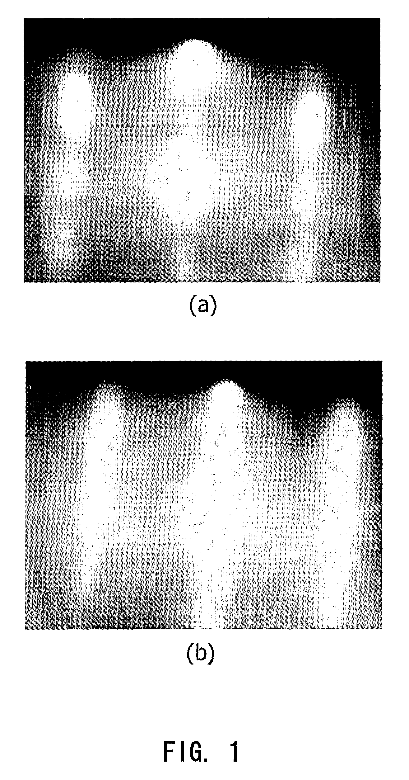
[0021]FIGS. 1A and 1B show RHEED patterns of a low-temperature buffer layer for deposition of a highly pure ZnO thin film using MBE. As shown in FIGS. 1A and 1B, in order to grow a ZnO thin film having high quality on the surface of the sapphire single-crystal substrate, the sapphire substrate is maintained at a relatively low temper...


PUM


Abstract

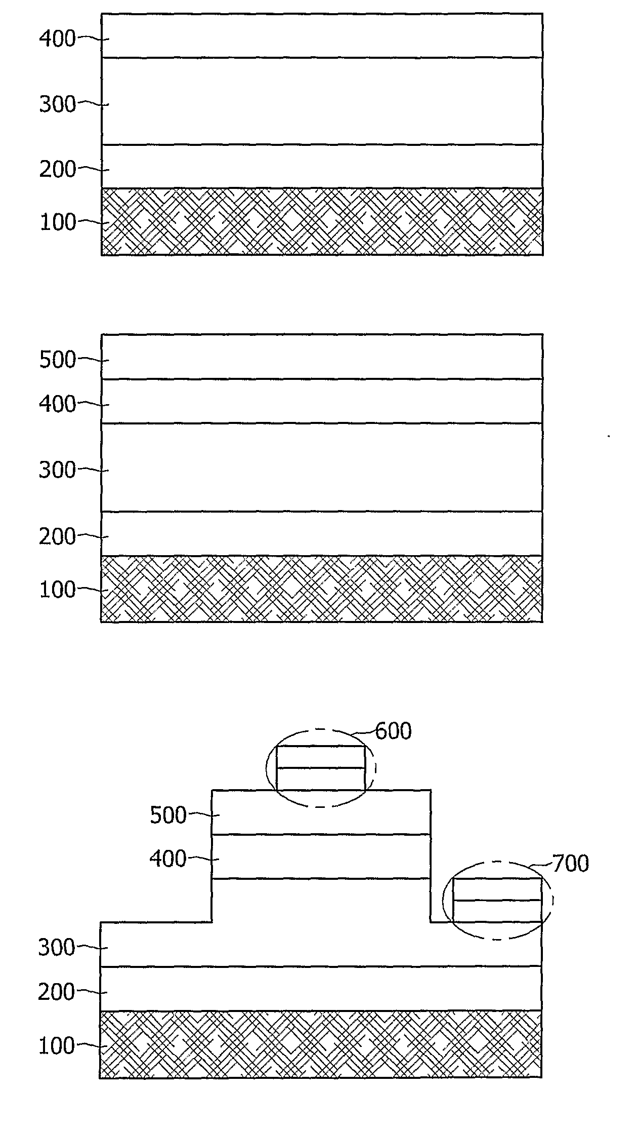
A method of fabricating a p-i-n type light emitting diode using p-type ZnO, and particularly, a technique for fabricating a p-type ZnO thin film doped with copper, a light emitting diode manufactured using the same, and its application to electrical and magnetic devices. The method of fabricating a p-i-n type light emitting diode using p-type ZnO includes depositing a low-temperature ZnO buffer layer on a sapphire single-crystal substrate, depositing an n-type gallium doped ZnO layer on the deposited low-temperature ZnO buffer layer, depositing an intrinsic ZnO thin film on the deposited n-type gallium doped ZnO layer, forming a p-type ZnO thin film layer on the deposited intrinsic ZnO thin film, forming a MESA structure on the p-type ZnO thin film layer through wet etching to obtain a diode structure, and subjecting the diode structure to post-heat treatment.

Description

TECHNICAL FIELD[0001]The present invention relates, generally, to a method of fabricating a p-i-n type light emitting diode using p-type ZnO, and more particularly, to a novel technique for fabricating a p-type ZnO thin film doped with copper, a light emitting diode (LED) manufactured using the same, and its application to electrical and magnetic devices.BACKGROUND ART[0002]In general, since ZnO has an optical bandgap of 3.37 eV near the UV region and a large exciton bonding energy of 60 meV at room temperature, it is receiving attention as a material for optical devices using excitons having higher light efficiency, compared to ZnSe (21 meV) or GaN (28 meV). Further, ZnO has optical gain of 300 cm−1, which is three times the 100 cm−1 of conventionally used GaN, and has saturation velocity (Vs) greater than GaN, and is thus preferably used for actual application to electrical devices. Furthermore, ZnO is known to have low threshold energy (Jth (W / cm2)) for lasing and therefore to be...

Claims


Application Information

Patent Timeline
IPC IPC(8): H01L21/00H01L33/12H01L33/28H01L33/36
CPCH01L33/0012H01L33/285H01L33/0095H01L33/0087
Inventor CHOI, WON-KOOKJUNG, YEON-SIK
Owner KOREA INST OF SCI & TECH
Learn More