Semiconductor Device

a technology of semiconductor devices and semiconductors, applied in semiconductor devices, semiconductor/solid-state device details, diodes, etc., can solve the problems of degrading electric characteristics, thermal runaway, and significantly limited performance of hbt operating with high power, and achieves high heat dissipation performance and inhibits the increase of chip area

Active Publication Date: 2008-09-25
RENESAS ELECTRONICS CORP
View PDF2 Cites 37 Cited by
  • Summary
  • Abstract
  • Description
  • Claims
  • Application Information

AI Technical Summary

Benefits of technology

[0054]According to the present invention, a semiconductor device having sufficiently high heat dissipation performance while inhibiting an increase in a chip area is achieved.

Problems solved by technology

Therefore, the performance of the HBT operating with high power is significantly limited by power consumed in the semiconductor device equipped with the HBT.
A positive feedback phenomenon in which the increase in the collector current incurs a further rise in temperature of the semiconductor element occurs, leading ultimately to a thermal runaway in some cases.
However, there is a problem of degrading electric characteristics if the value of the ballast resistance is high.
Furthermore, in the case of the FET, the mobility drops if the channel temperature rises due to self-heating of the semiconductor element.
Due to the increase in on-resistance, a problem of degradation of the output power and efficiency arises.
If the gate width or the emitter area is simply increased, various problems of degrading the output efficiency, increasing the chip area, and so on, and therefore a large number of semiconductor elements as fundamental units are arranged side by side at certain intervals and operated in parallel.
Thus, the unit semiconductor element at the central part of the multi-cell structure has a temperature higher than that of the unit semiconductor element at the peripheral part of a semiconductor substrate, and a temperature unbalance occurs to cause a problem of degrading electric characteristics, and further, in the HBT, there is a problem of being susceptible to a thermal runaway by positive feedback of generated heat.
However, the method of reducing the thickness of a substrate has a problem of degradation of the mechanical strength of a chip.
For example, when a compound semiconductor having relatively small thermal conductivity, such as GaAs, is used as a substrate, the thermal resistance cannot be reduced effectively unless the thickness of the substrate is reduced to 50 μm or less, but the mechanical strength of a chip is not sufficiently with such a thin substrate.

Method used


Image

  • Semiconductor Device
  • Semiconductor Device
  • Semiconductor Device

Examples


first embodiment

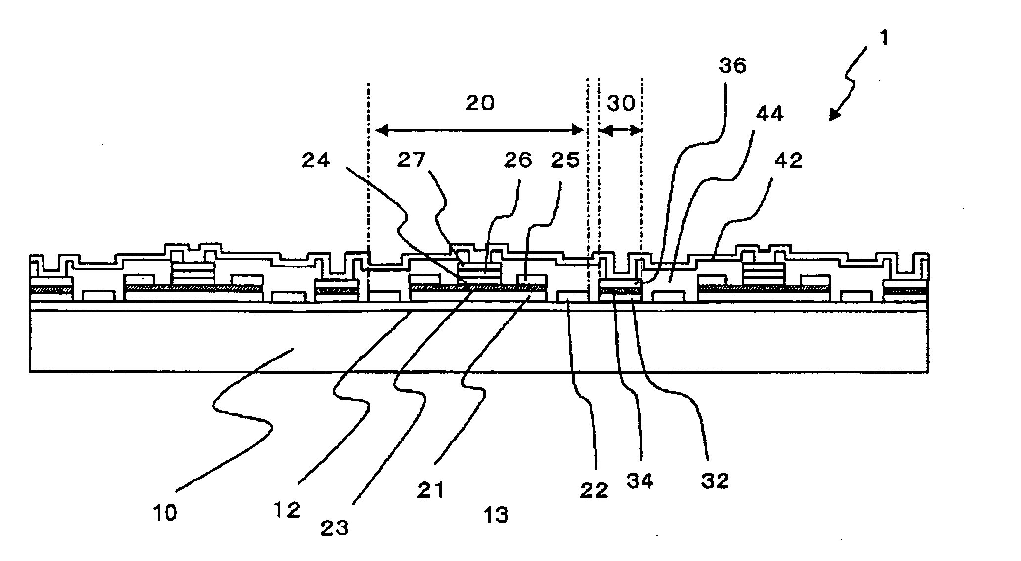
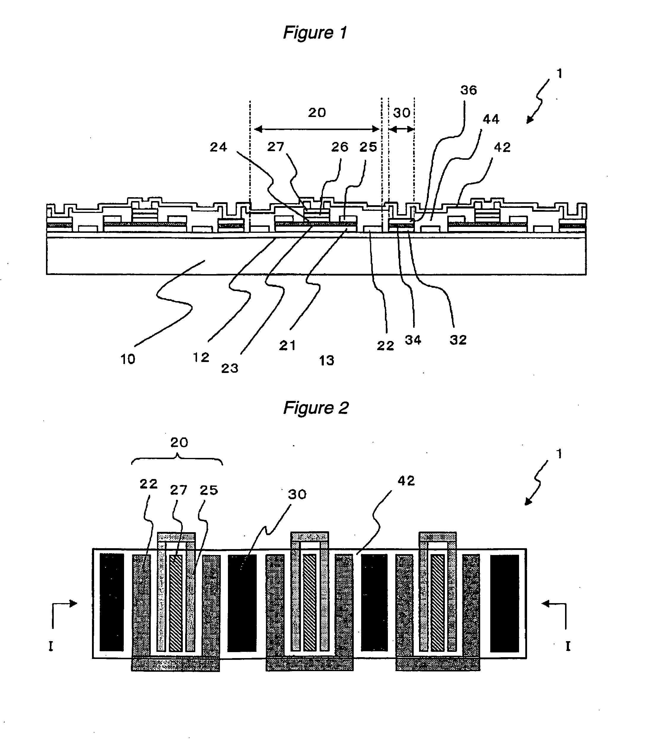
[0113]FIG. 1 is a sectional view showing a first embodiment of the semiconductor device according to the present invention. FIG. 2 is a plan view showing the first embodiment of the semiconductor device according to the present invention. FIG. 1 shows a cross-section taken along line I-I of FIG. 2.

[0114]Semiconductor device 1 of this embodiment is so called a high-output power semiconductor device of multi-cell structure having a plurality of n-p-n type HBTs formed on a semi-insulating semiconductor substrate. This embodiment is described with an example of using a semi-insulating semiconductor substrate as a semiconductor substrate, but an n type semiconductor substrate may be used or a p-n-p type HBT may be used as a matter of course.

[0115]Semiconductor device 1 shown in FIG. 1 comprises sub-collector layer 12 formed on the (001) plane of semi-insulating semiconductor substrate 10, HBTs 20 as unit semiconductor elements one-dimensionally and alternately arranged on sub-collector l...

second embodiment

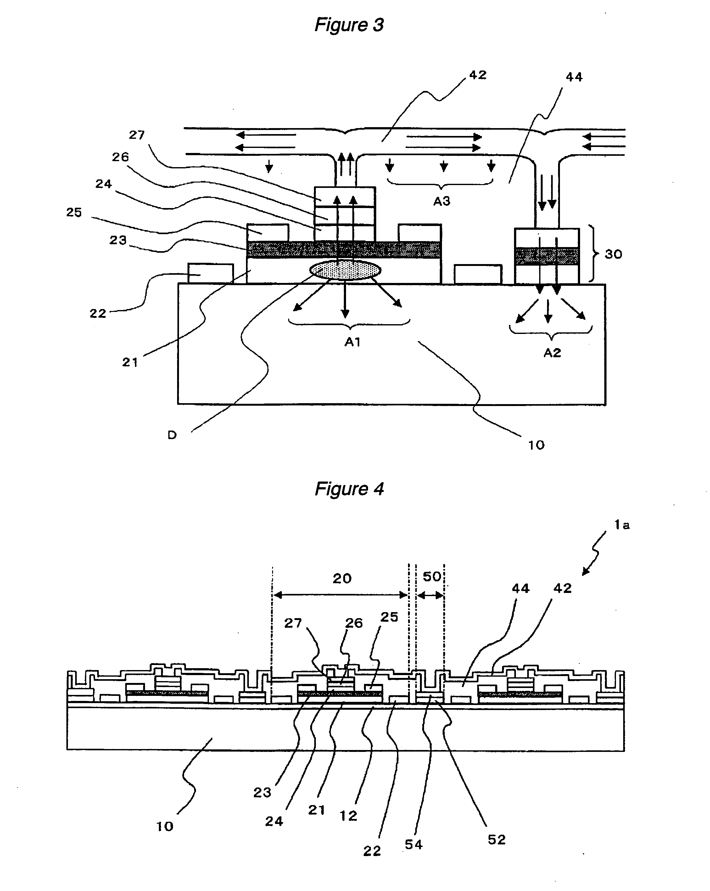
[0164]FIG. 4 is a cross-sectional view showing a second embodiment of the semiconductor device according to the present invention. Semiconductor device 1a is different from semiconductor device 1 in the configuration of diode 50. Other configurations of semiconductor device 1a are same as those of semiconductor device 1. Diode 50 is a Schottky junction diode constituted by n type layer 42 and Schottky electrode 54 stacked in this order on sub-collector layer 12, and works for both the heat dissipating means and protection diode. Like n type layer 32 of FIG. 1, n type layer 52 has a composition same as that of collector layer 21 of HBT 20. Schottky electrode 54 is connected to emitter electrode 27 via common emitter wiring 42.

[0165]As a Schottky metal, a metal such as titanium, aluminum or tantalum may be used. When titanium is used as a Schottky metal, the configuration of Schottky electrode 54 may use, for example, a Ti / Pt / Au electrode.

[0166]Since the HBT of this embodiment is an n...

third embodiment

[0171]FIG. 5 is a cross-sectional view showing a third embodiment of the semiconductor device according to the present invention. FIG. 6 is a plan view showing the third embodiment of the semiconductor device according to the present invention. In semiconductor device 2, a plurality of HBTs 20 and a plurality of heat dissipating means 60 are one-dimensionally alternately arranged on semiconductor substrate 10. The configuration of HBT 20 is similar to that shown in FIG. 1.

[0172]Heat dissipating means 60 is constituted by metal film 62 formed on sub-collector layer 12 and insulating film 44 on metal film 62. Insulating film 44 is similar to the insulating film shown in FIG. 1. Namely, a portion of insulating film 44 provided on metal film 62 works as a part of heat dissipating means 60. Insulating film 44 of heat dissipating means 60 is connected to emitter electrode 27 of HBT 20 via common emitter wiring 42. In other words, insulating film 44 is interposed between metal film 62 and ...


PUM


Abstract

A semiconductor device having sufficiently high heat dissipation performance while inhibiting an increase in the area of a chip is provided. In semiconductor device 1, a plurality of HBTs 20 and a plurality of diodes 30 are one-dimensionally and alternately arranged on semiconductor substrate 10. Anode electrode 36 of diode 30 is connected to emitter electrode 27 of HBT 20 via common emitter wiring 42. Diode 30 works as heat dissipating elements dissipating to semiconductor substrate 10 the heat transmitted through common emitter wiring 42 from emitter electrode 27, and also works as a protection diode connected in parallel between an emitter and a collector of HBT 20.

Description

TECHNICAL FIELD[0001]The present invention relates to a semiconductor device.BACKGROUND ART[0002]A high-frequency power amplifier (hereinafter abbreviated as PA) that is used in a mobile communication terminal such as a mobile phone is required to have a high output so that satisfactory communications are possible even at a location distant from a communication relay point.[0003]For semiconductor devices that are used in the high-frequency power amplifier, high-output semiconductor devices (power transistors) employing a plurality of semiconductor elements having as a fundamental unit a III-V group compound semiconductor type metal semiconductor field effect transistor (hereinafter abbreviated as MESFET) or an element called an HEMT (high electron mobility transistor (hereinafter abbreviated as HEMT)) having improved high-frequency characteristics and noise characteristics of the MESFET (hereinafter referred to as FET with MESFET and HEMT in combination in some cases), or hetero-jun...

Claims


Application Information

Patent Timeline
Patent Type & Authority Applications(United States)
IPC IPC(8): H01L29/73H01L23/34H01L21/3205H01L21/331H01L27/06H01L27/095H01L29/47H01L29/737H01L29/866H01L29/872
CPCH01L23/367H01L27/0605H01L27/0664H01L29/66318H01L2924/0002H01L29/7371H01L2924/00
Inventor KURODA, NAOTAKATANOMURA, MASAHIROKUROSAWA, NAOTO
Owner RENESAS ELECTRONICS CORP
Why Eureka
Try Eureka