
Wiring board, mounting structure for electronic components, and semiconductor device

a technology for mounting structures and electronic components, applied in the direction of resist details, electrical apparatus contruction details, association of printed circuit non-printed electric components, etc., can solve problems such as high probability of difficulty, device characteristics degradation, and operating failure of semiconductor devices

Active Publication Date: 2008-09-18
SOCIONEXT INC
View PDF9 Cites 14 Cited by
  • Summary
  • Abstract
  • Description
  • Claims
  • Application Information

AI Technical Summary

Problems solved by technology

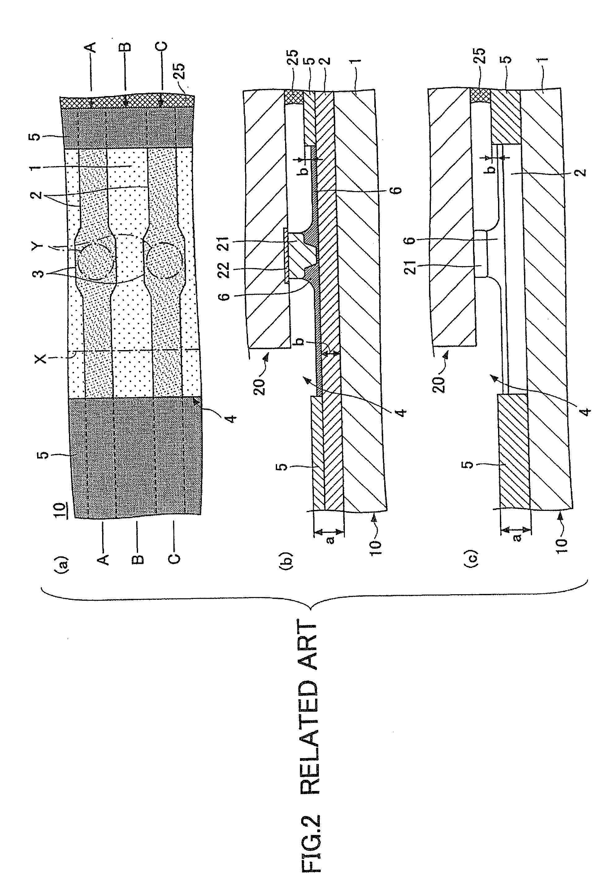
Further, when the void B is formed near the convex shaped external connecting terminals 21 of the semiconductor 20, the moisture or impurities contained in the void B can affect a leakage current flowing between the adjacent terminals of the convex shaped external connecting terminals 21, and it may cause a degradation of the device characteristics or operating failure of the semiconductor device.
Further, even in the conventional case when such difficulty does not arise from the size of the void B, such difficulty is highly likely to arise when the pitch of plural convex external connecting terminals 21 of the semiconductor element 20 becomes smaller.

Method used


Image

  • Wiring board, mounting structure for electronic components, and semiconductor device
  • Wiring board, mounting structure for electronic components, and semiconductor device
  • Wiring board, mounting structure for electronic components, and semiconductor device

Examples


first embodiment

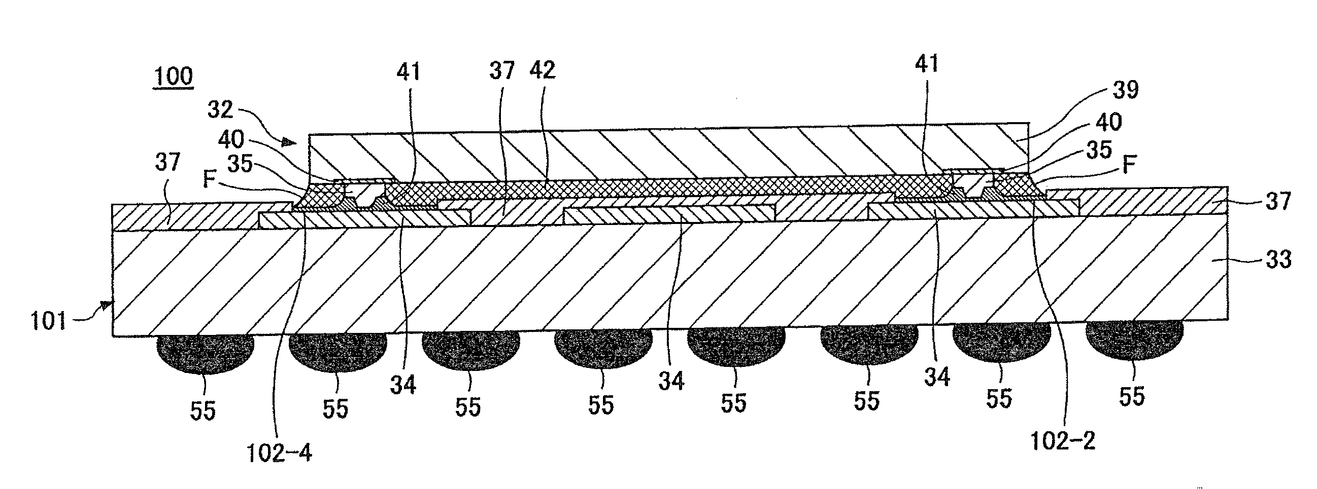
[0075]First, FIG. 6 is an illustrative drawing related to the present invention and showing major portions of a structure for a semiconductor element mounted onto a wiring board.

[0076]Referring to FIG. 6, a semiconductor device 30 includes a semiconductor integrated circuit device (“semiconductor element”) 32 flip-chip (face-down) mounted on and connected to one main (top) surface of a wiring board 31.

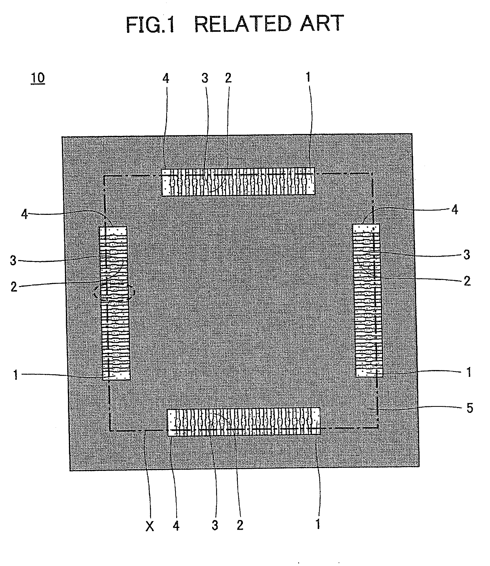
[0077]For a detailed description of the structure of the wiring board 31, refer to FIG. 7 as well. FIG. 7 is an illustrative drawing showing a cut-away plan view of the structure of the wiring board of FIG. 6. Then, a dashed line X in FIG. 7 indicates the outer area of the semiconductor element 32 (see FIG. 6) to be mounted faced down on the wiring board 31.

[0078]The wiring board 31 is provided with a substrate material 33 that is glass epoxy resin, glass-BT (glass-bismaleimide-triazine), polyimide such as organic insulating resin, or inorganic matter such as ceramic or glass, and the ...

second embodiment

[0166]However, the present invention is not limited to such an example, and it is applicable for the following case as well; after a semiconductor element is mounted on and connected to a wiring board, an underfill material is coated near the peripheral region of the semiconductor element on the wiring board and flows all over the area of the semiconductor element, and the underfill material is solidified by succeeding heating. Thus it is applicable a wiring board using such a method. This is explained as the present invention in the following.

[0167]FIG. 19 shows a plan view of the wiring board related to the second embodiment of the present invention. In FIG. 19, the identical parts referred in FIG. 7 are assigned the identical numbers, and the explanations are omitted. Further, for FIG. 19, the alternate long and short dash line X indicates the peripheral region of the wiring board 10 on which a semiconductor element is mounted face down (in a face-down manner).

[0168]Referring to ...


PUM


Abstract

A wiring board includes a main surface where an electronic component is mounted in a face-down manner so that a surface of the electronic component having plurality of external connecting terminals faces the main surface of the wiring board, the electronic component being fixed to the wiring board by an adhesive; an insulating layer formed on the main surface where the electronic component is mounted; an opening part formed in the insulating layer so that a plurality of adjacent wiring patterns are commonly and partially opened, the adjacent wiring patterns having electrodes where electrodes of the electronic component are connected; wherein an outer periphery of the opening part situated at a center side of the wiring board is formed in an oblique direction against extending directions of the wiring patters.

Description

BACKGROUND OF THE INVENTION[0001]1. Field of the Invention[0002]The present invention generally relates to wiring boards, a mounting structure for electronic components, and semiconductor devices, and more specifically, to an wiring board for mounting electronic components such as for a semiconductor device, the mounting structure for the electronic components, and the semiconductor device.[0003]2. Description of the Related Art[0004]There is a semiconductor device which includes a substrate material that is insulating resin such as glass epoxy resin or the like, a wiring board having a selectively provided conducting layer such as copper (Cu), an external connecting terminal having plural projections (projection form) named as bumps arranged in line on a main plane of a semiconductor integrated circuit device (named as semiconductor element) connected to the conducting layer, and the other main plane of the wiring board having another external connecting terminal selectively provid...

Claims


Application Information

Patent Timeline
Patent Type & Authority Applications(United States)
IPC IPC(8): H01L23/12H05K7/14
CPCH01L21/563H01L23/49816H01L23/49838H01L24/16H01L24/29H01L24/32H01L24/75H01L24/81H01L24/83H01L24/92H01L2224/1134H01L2224/131H01L2224/13144H01L2224/13147H01L2224/16225H01L2224/73204H01L2224/75H01L2224/75251H01L2224/75252H01L2224/75743H01L2224/81191H01L2224/81203H01L2224/81801H01L2224/838H01L2224/92225H01L2924/01013H01L2924/01029H01L2924/01033H01L2924/01047H01L2924/01078H01L2924/01079H01L2924/01082H01L2924/09701H01L2924/10329H01L2924/14H01L2924/15311H01L2924/19041H01L2924/19043H05K3/305H05K3/3452H05K2201/0989H05K2201/10674H05K2201/10977H05K2203/0594H01L2224/2919H01L2924/00013H01L2924/01005H01L2924/01006H01L2924/0105H01L2924/01075H01L2924/014H01L2924/0665H01L2924/0132H01L2924/0133H01L2924/1579H01L2224/92125H01L2224/32225H01L2224/29111H01L2224/83192H01L2924/00014H01L2224/13099H01L2924/00H01L2924/00012H01L2224/0401H01L2224/0554H01L2224/0557H01L2224/05571H01L2224/05573H01L2224/05624H01L2224/05647H01L2224/13007H01L2224/16237H01L2224/81385H01L2924/013H01L2224/05599H01L2224/0555H01L2224/0556H01L23/12H01L23/48H05K1/18
Inventor NISHIMURA, TAKAOKUMAGAYA, YOSHIKAZU
Owner SOCIONEXT INC
Learn More