
Embedded capacitor

a capacitor and embedded technology, applied in the field of embedded capacitors, can solve the problems of excessively large area of real estate, high real-estate usage, and low capacitance values of embedding capacitors, and achieve the effects of minimizing real-estate usage, enhancing capacitance density in printed circuit boards, and high capacitan

Inactive Publication Date: 2008-09-11
DELPHI TECH INC
View PDF2 Cites 8 Cited by
  • Summary
  • Abstract
  • Description
  • Claims
  • Application Information

AI Technical Summary

Benefits of technology

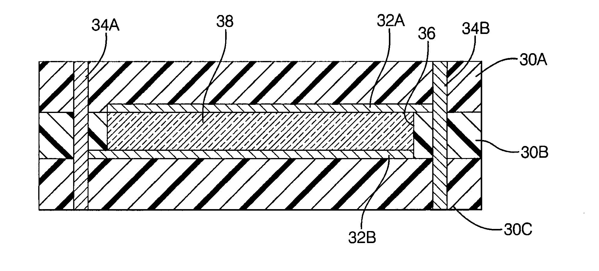
[0007]An embedded capacitor method and system is provided for printed circuit boards. The capacitor structure is embedded in a substrate, provides a high capacitance, and yet forms an advantageous planar surface topography. The embedded capacitor minimizes real-estate usage by occupying limited space and enhancing capacitance density in a printed circuit board. This in turn results in an overall reduced circuit size and improved circuit performance. The capacitor structure may also be embedded in a multilayer substrate providing even greater capacitance, and yet the capacitor structure maintains a planar surface topography.

Problems solved by technology

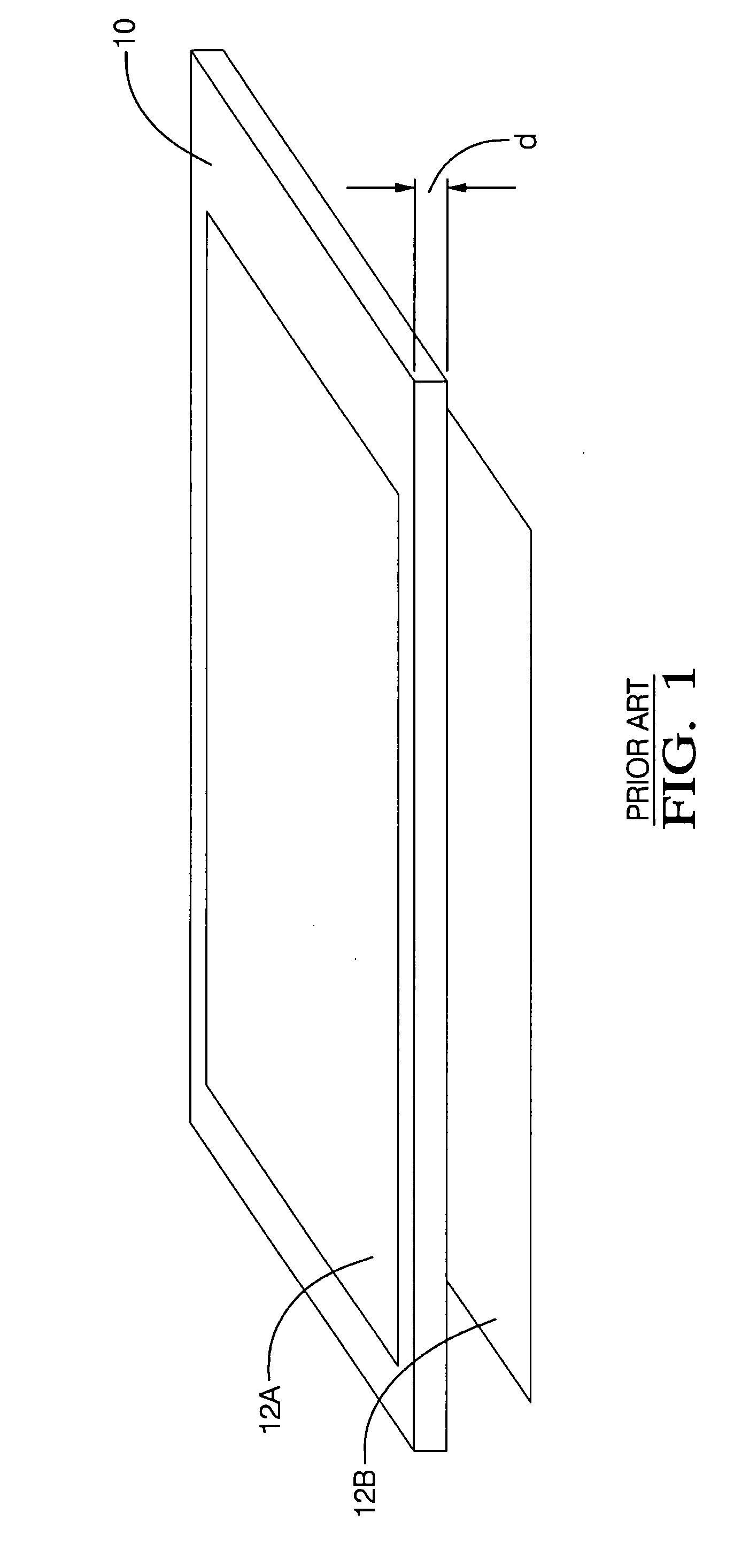
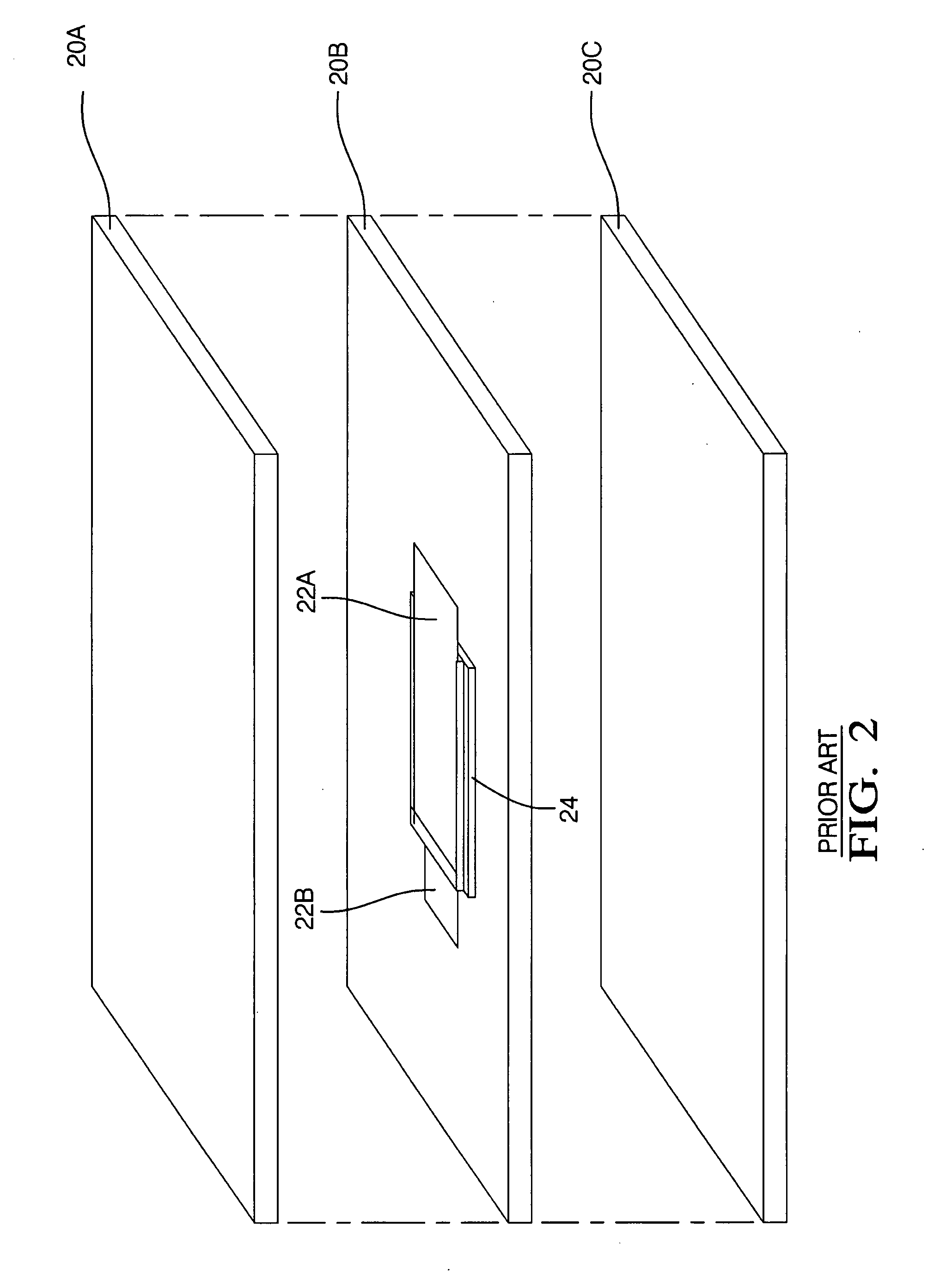
Since the design of smaller and denser printed circuit boards is approaching a practical limit for today's technology, circuit designers must maximize real-estate usage.
Embedding capacitors, however, are characteristically limited to low capacitance values due to design and manufacturing constraints.
This process presents a limitation in that it is only useful for low value capacitors in the range of about 0.01 to 0.1 nanofarads (nF).
Further, an excessively large area of real estate is required to provide even a low value capacitance.
However, when the device is fired, an undesirable surface topography results.
A non-planar bump results, which presents its own limitations and problems.

Method used


Image

  • Embedded capacitor
  • Embedded capacitor
  • Embedded capacitor

Examples


Embodiment Construction

[0026]Exemplary embodiments are described with reference to specific configurations. Those of ordinary skill in the art will appreciate that various changes and modifications can be made while remaining within the scope of the appended claims. Additionally, well-known elements, devices, components, methods, process steps and the like may not be set forth in detail in order to avoid obscuring the invention. Further, unless indicated to the contrary, the numerical values set forth in the following specification and claims are approximations that may vary depending upon the desired characteristics sought to be obtained by the present invention.

[0027]A system and method are described herein for providing an embedded capacitor for printed circuit boards. The capacitor structure is embedded in an insulator substrate, provides a high capacitance, and yet forms an advantageous planar surface topography. The embedded capacitor minimizes real-estate usage and enhances capacitance density in a...


PUM

PropertyMeasurementUnit
Fractionaaaaaaaaaa
Fractionaaaaaaaaaa
Diameteraaaaaaaaaa

Abstract

An embedded capacitor method and system is provided for printed circuit boards. The capacitor structure is embedded within an insulator substrate, minimizes real-estate usage, provides a high capacitance, enhances capacitance density, and yet forms an advantageous planar surface topography. A cavity is defined within and contained by an insulator substrate layer, and a dielectric material at least partially fills the cavity. The dielectric material is connected to an electrical conductor, and vias are used for interconnections and traces. In an aspect, a plurality of stacked insulator substrate layers define a plurality of cavities filled with the dielectric material, providing even greater capacitance. In another aspect, an array of cavities is formed in the insulator substrate layer. The embedded capacitor can be employed within numerous systems that utilize capacitors including automotive electronics such as a pressure sensor, an engine control module, a transmission controller, and radio systems including satellite radio devices.

Description

FIELD OF THE INVENTION[0001]The invention relates generally to a capacitor structure, and more particularly to an embedded and planar capacitor structure in a multilayer substrate providing a high value capacitance.BACKGROUND OF THE INVENTION[0002]The demand for miniaturized electronic devices is ever intensifying with both circuit density and the density of components per unit area significantly increasing. The number of components employed has risen exponentially, necessitating a shrinkage of component size. Since the design of smaller and denser printed circuit boards is approaching a practical limit for today's technology, circuit designers must maximize real-estate usage. In the case of surface mounting, components are added if they are exceptionally small. Alternatively, components can be added if they are buried within inner layers, as in the case of vertical stacking.[0003]Passive circuit components embedded in printed circuit boards (PCB) and thick film resistor and dielect...

Claims


Application Information

Patent Timeline
IPC IPC(8): H01G7/04
CPCH05K1/0306H05K1/0313H05K1/162H05K3/429Y10T29/435H05K2201/0187H05K2201/0209H05K2201/09763H05K3/4611
Inventor BERLIN, CARL W.SARMA, DWADASI H. R.CHAPPELL, WILLIAM J.HOPPENJANS, ERIC E.
Owner DELPHI TECH INC
Learn More