Optical waveguide sensor and method of manufacture

a technology of optical waveguide and environmental sensor, which is applied in the field of optical waveguide environmental sensor, can solve the problems of limiting affecting the production run of expensive compositions, and affecting the usefulness of such sensors, so as to minimize the detection response time, reduce the response time, and maximize the exposure of the side

Inactive Publication Date: 2008-08-28
CORNING INC
View PDF9 Cites 11 Cited by
  • Summary
  • Abstract
  • Description
  • Claims
  • Application Information

AI Technical Summary

Benefits of technology

[0011]The elongated opening preferably runs most or all of the length of the waveguide in order to maximize exposure of the side of the hollow core portion to the ambient environment and to minimize the response time of detection, preferably to seconds or less. The optical waveguide may have a plurality of such elongated openings, each of which operates to expose a side of the hollow core portion to the ambient environment and to further reduce response time. To eliminate optical birefringence, the plurality of elongated openings may be symmetrically disposed around the cladding.
[0012]The elongated opening may take the form of a slot-like groove having parallel side walls. Such a slot-like opening may extend through only through one side of the cladding to the hollow core portion, or completely through the cladding thereby exposing two sides of the hollow core portion. Alternatively, the elongated opening may be formed by the removal of a wedge-shaped section of cladding such that the side walls of the opening are disposed at an angle to one another when the waveguide is viewed in cross section. Finally, the elongated opening may also be formed by the removal of a flat-sided section of cladding such that the side walls of the elongated opening are co-planar, thus giving the optical fiber sensor a “D” shaped profile when viewed in cross section. When the elongated opening is formed in this last-described manner, the optical fiber is preferably bent around a radius in a spiral configuration with the flat side of the “D” shaped profile on the inside of the bend in order to reduce light losses in the resulting fiber, as the optical mode conducted through the resulting ridge waveguide is more weakly bound by such an open configuration of the hollow core portion.
[0013]The optical fiber sensor of the invention may also have multiple hollow cores which are preferably optically coupled to one another. For example, in such embodiment, one or all of the hollow core portions may be exposed to the ambient environment by one or more elongated openings. For example, in such a sensor one hole may be isolated from the environment to act as a reference optical path, while the other core or cores may be exposed to the environment, there-by producing an interferometric sensor in which light in the reference optical path will interfere with light in the sensing optical path yielding a signal that is related to the concentration of the target gas or liquid species. Such a differential or interferometric sensor according to some embodiments of the present invention can remove the effect of other environmental changes such as temperature and pressure.

Problems solved by technology

Unfortunately, there are a number of shortcomings associated with such prior art optical fiber environmental sensors.
Such restricted access to the hollow core of the sensor fiber results in a relatively long response time for such a sensor to detect a particular “target” gas or liquid.
Such a long response time substantially limits the usefulness of such sensors in many applications, such as chemical manufacturing applications, where a 2 minute delay may result in the irretrievable ruin of a production run of an expensive composition.
Thus far, no satisfactory way to shorten the response time for such sensors has been found.
Of course, the length of the optical fiber sensor could be shortened, but such shortening not only reduces the sensitivity of the sensor (as sensitivity is proportional to the total volume of the hollow core) but also makes it apt to generate false positives (as a single tendril of cigarette smoke curling around a 1 cm smoke detector may trigger it).
However, such capillary tube optical waveguides have high light losses of over 1 dB / m, which imposes practical limits on the length of such a sensor, and are also relatively stiff and inflexible, which prevents them from being installed in space-limited situations where a sharp bending or tight coiling of the sensor is desired.
However, such coated capillary tubes would be substantially more expensive to manufacture than drawn optical fibers.
Additionally, the losses would still be greater than 0.5 dB / m, and the problems associated with stiffness and inflexibility would remain.
While such a solution may shorten the response time of the fiber sensor, the resulting response time would still be unacceptably long due the fact that access to the hollow core is still quite limited.
Additionally, there is a concern in the prior art that such radially-oriented side openings create “light leaks” that limit the number of side openings that can be fabricated in such a fiber before the resulting losses become unacceptably high.
Clearly, what is needed is an optical waveguide environmental sensor that maintains the low losses, flexibility and ease of manufacture associated with optical fibers, but which substantially reduces the response time associated with fiber-based environmental sensors that rely upon a relatively small number of end or side holes to expose the hollow core of the fiber to the ambient environment.

Method used


Image

  • Optical waveguide sensor and method of manufacture
  • Optical waveguide sensor and method of manufacture
  • Optical waveguide sensor and method of manufacture

Examples


Embodiment Construction

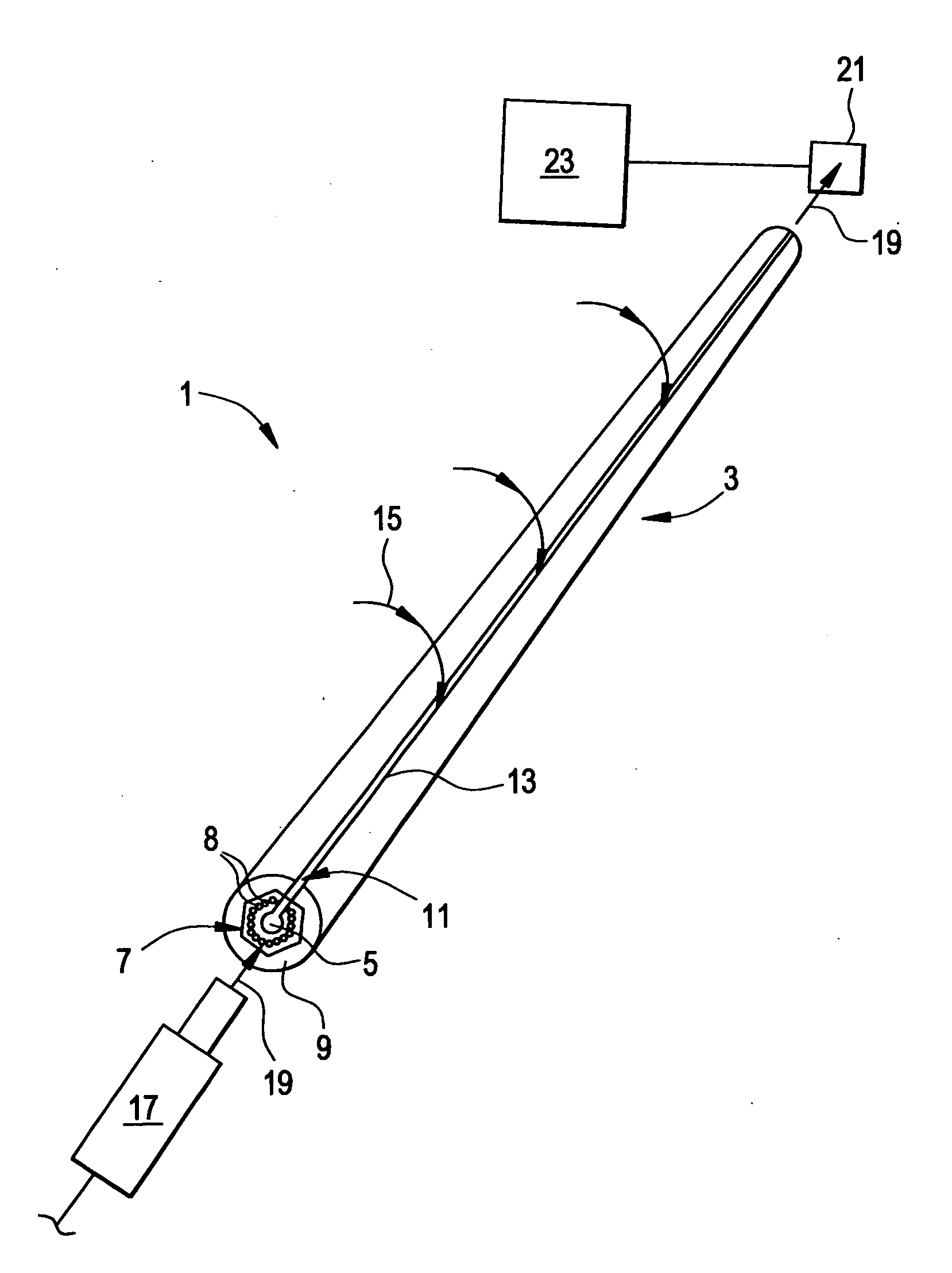
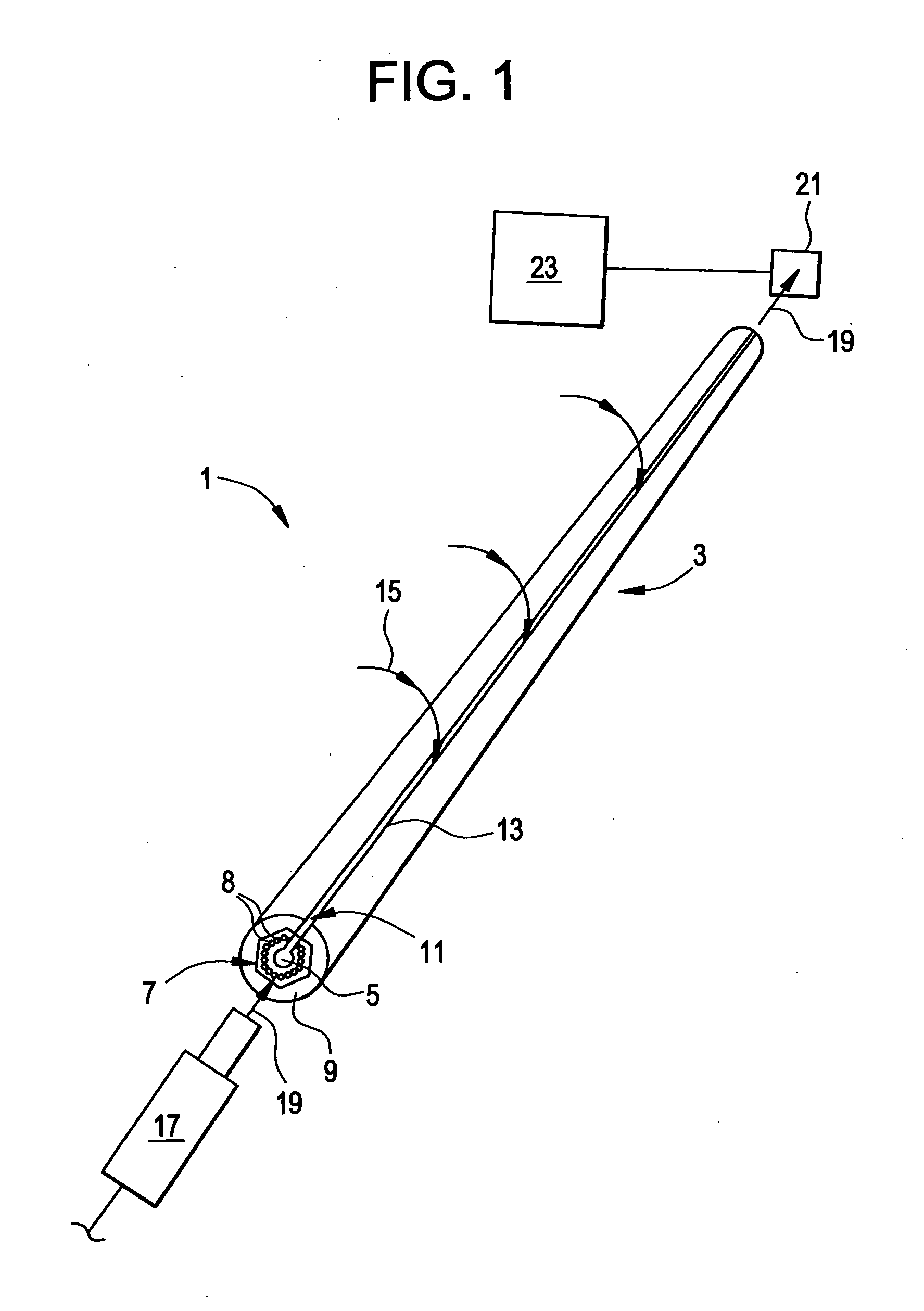
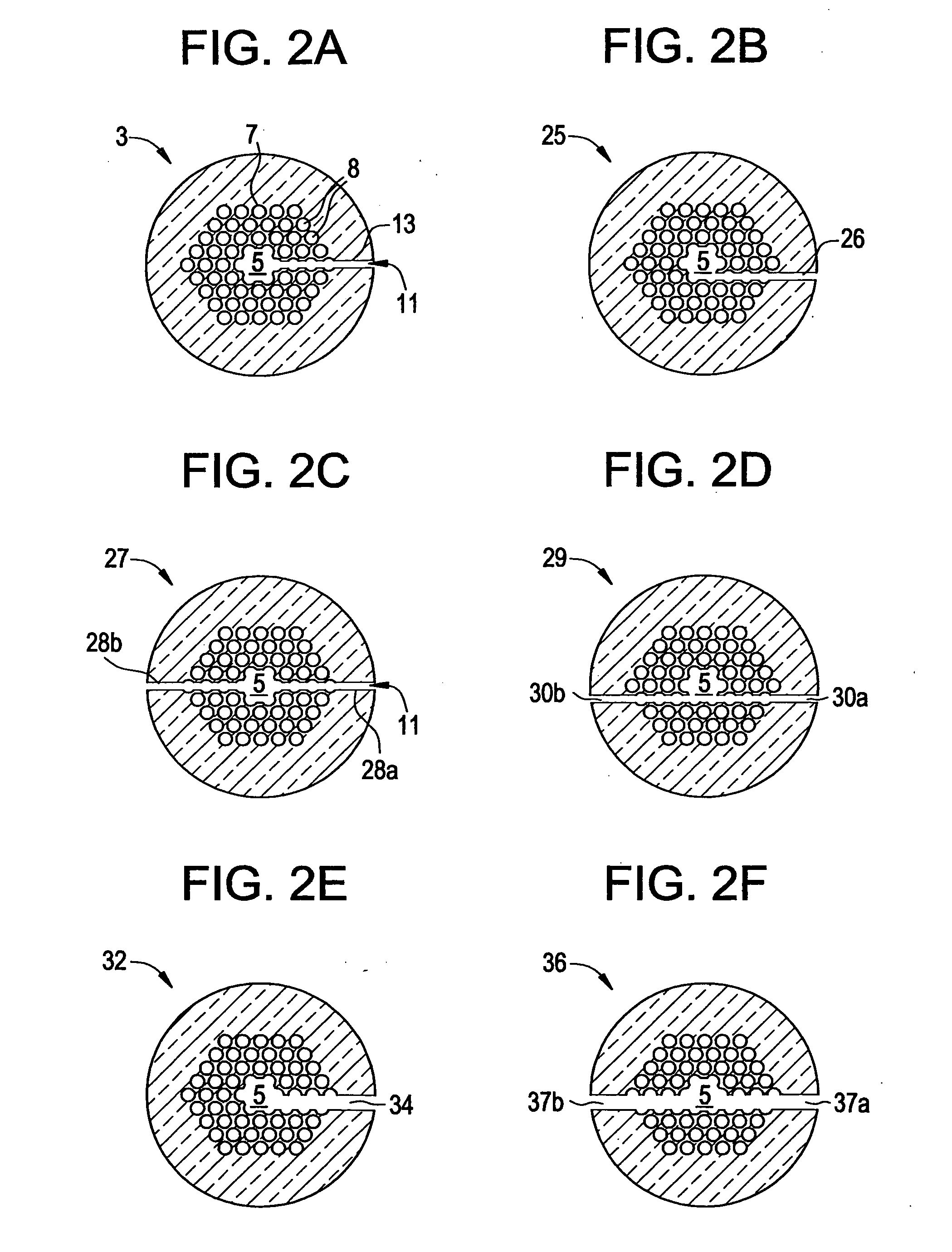
[0032]With reference now to FIG. 1, wherein like numerals designate like components throughout all the several figures, the optical waveguide sensor 1 of the invention preferably comprises a photonic band gap fiber 3 having a lattice-type microstructure 7 hereinafter referred to as cladding 7. The cladding 7 includes a pattern of different light conducting materials having different indexes of refraction, such as a pattern of air holes 8 (shown in FIGS. 2A-4F) in the silica present in the center of the fiber 3. Alternatively, the cladding 7 may be formed from an alternating pattern of two different solid light conducting materials, such as two different types of glasses, or a glass and a plastic material. Finally, the cladding 7 may be formed from alternating layers of such materials, so long as the differences in the index of refraction between the two materials effectively creates a “forbidden zone” that confines a least one optical mode within the hollow core 5. The cladding 7 is...


PUM

PropertyMeasurementUnit
lengthaaaaaaaaaa
diameteraaaaaaaaaa
radiusaaaaaaaaaa

Abstract

An optical waveguide environmental sensor is provided that is capable of detecting a target gas or liquid in the ambient environment in an advantageously short period of time. The waveguide is preferably in the form of an optical fiber having a cladding that contains a photonic band gap structure which in turn envelopes a light conducting, hollow core portion. The cladding further includes at least one elongated side opening that preferably extends the entire length of the fiber and exposes said hollow core portion to the ambient environment, which provides broad and nearly immediate access of the core portion to gases and liquids in the ambient environment, thereby minimizing sensor response time. The ambient gases or liquids filling the hollow core portion and elongated opening function as a ridge and slab, respectively, of an optical ridge waveguide that effectively supports at least one bound optical mode.

Description

[0001]This is a divisional application of U.S. application Ser. No. 11 / 711,199, filed Feb. 27, 2007, entitled “Optical Waveguide Environmental Sensor and Method of Manufacture”.FIELD OF THE INVENTION[0002]This invention generally relates to an optical waveguide environmental sensor and the method of manufacturing the same, and is specifically concerned with such a sensor in the form of a photonic band gap fiber having an elongated side opening that exposes its hollow core to the ambient environment.BACKGROUND OF THE INVENTION[0003]Environmental sensors in the form of optical fibers having a hollow core are known in the prior art. The hollow core of the fibers used for such sensors typically conducts light by way of a photonic band gap structure (PBG) surrounding the hollow core having a “forbidden frequency range” which corresponds to the wavelength of the light transmitted through the fiber, although hollow core fibers that conduct light via total internal reflection (TIR) for a sp...

Claims


Application Information

Patent Timeline
Patent Type & Authority Applications(United States)
IPC IPC(8): C03B37/023G02B6/028G02B6/032
CPCG01N21/0303G01N21/3504G01N21/65G02B6/02385G02B6/02328G02B6/02361G01N2021/653
Inventor GALLAGHER, MICHAEL THOMASKOCH, KARL WILLIAMWILLIAMS, ELLEN MARIE KOSIKWEST, JAMES ANDREW
Owner CORNING INC
Why Eureka
Try Eureka