Chemical mechanical polishing pad
a technology of mechanical polishing and polishing pads, which is applied in the field of polishing pads, can solve the problems of increasing the complexity of the manufacturing of these semiconductor devices, and increasing the cost of cmp consumables,
- Summary
- Abstract
- Description
- Claims
- Application Information
AI Technical Summary
Benefits of technology
Problems solved by technology
Method used
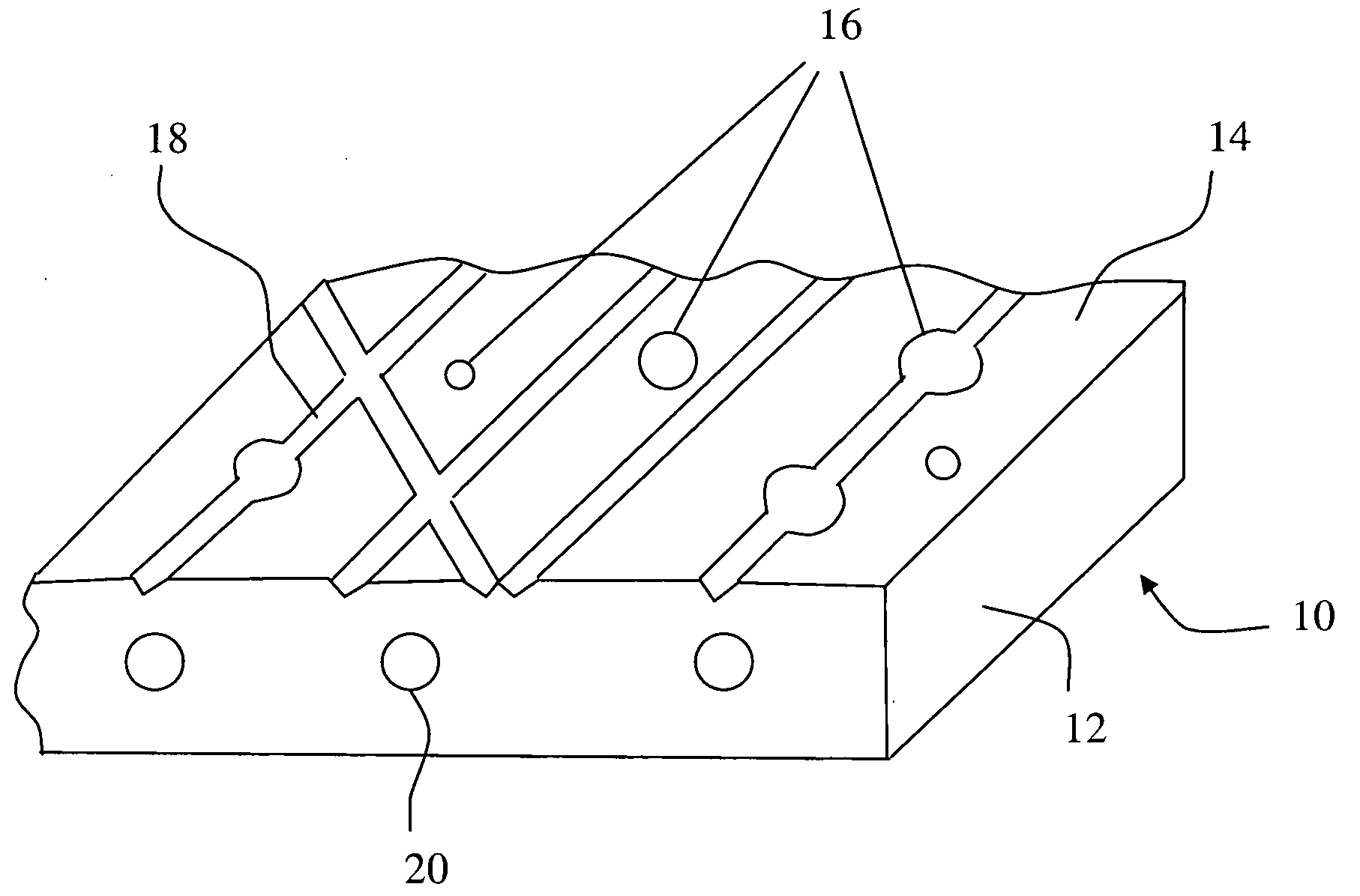
Image


Examples
example 1
[0045]The polymeric pad materials were prepared by mixing various amounts of isocyanates as urethane prepolymers with 4,4′-methylene-bis-o-chloroaniline [MBCA] at 50° C. for the prepolymer and 116° C. for MBCA. In particular, various toluene diiosocyanate [TDI] with polytetramethylene ether glycol [PTMEG] prepolymers provided polishing pads with different properties. The urethane / polyfunctional amine mixture was mixed with the hollow polymeric microspheres (EXPANCEL® 551DE20d60 or 551DE40d42 manufactured by AkzoNobel) either before or after mixing the prepolymer with the chain extender. The microspheres had a weight average diameter of 15 to 50 μm, with a range of 5 to 200 μm, and were blended at approximately 3,600 rpm using a high shear mixer to evenly distribute the microspheres in the mixture. The final mixture was transferred to a mold and permitted to gel for about 15 minutes.
[0046]The mold was then placed in a curing oven and cured with a cycle as follows: thirty minutes ramp...
example 2
[0050]The data in Table 4 represents dishing performance over a range of oxide isolation trench widths for experimental pad formulations that contain a range of pore volume percentages. The patterned wafers used to generate the data for all pads types utilized an MIT 864 mask pattern. This pattern includes HDP oxide trench features of various pitches and densities. The equipment, methodology, processes and procedures used on the experimental pads which polished the MIT 864 wafers, were the same as those described in conjunction with the data in Table 3 above. The dishing was calculated by measuring the remaining oxide thickness in the trenches specified in Table 4. These measurements were made on the KLA-Tencor FX200 thin film metrology tool.
TABLE 444 μm*44 μm*44 μm*180 μm**Diamond180 μm**Diamond180 μm**DiamondDiamond100 μmDiamond500 μmDiamondPore50 μm line50 μmline100 μmline500 μmFormulationvol, %(Å)(Å)(Å)(Å)(Å)(Å)119194336316570402897435224371404595547883611237109360268535355A3225...
example 3
[0053]Tables 5A and 5B include data which illustrates how varying the formulation factors of stoichiometry, pore size and pore volume percentage, in conjunction with the 44 μm conditioner, significantly improve dishing performance over an analogous pad conditioned with a more aggressive 180 μm diamond configuration. Polishing conditions, equipment and protocol as well as slurry and wafer type, used in generating the data below were the same as those described above for the data in Tables 3 and 4.
TABLE 5APore50 μm line100 μm line500 μm linePore sizeVolumeDishing*Dishing*Dishing*FormulationStoichiometry(μm)(%)(Å)(Å)(Å)1105201914225449521054019−53118B85404177138528C852041038193*Dishing represents result of subtracting 44 μm dishing value from 180 μm dishing value.
TABLE 5B50 μm line100 μm line500 μm line50 μm line100 μm line500 μm lineDishing*Dishing*Dishing*Dishing**Dishing**Dishing**Formulation(Å)(Å)(Å)(Å)(Å)(Å)11943164023365708972318485651313516669B2445115813216491109C259532695259570...
PUM
 Abstract
Description
Claims
Application Information
 - R&D
- Intellectual Property
- Life Sciences
- Materials
- Tech Scout
- Unparalleled Data Quality
- Higher Quality Content
- 60% Fewer Hallucinations
Browse by: Latest US Patents, China's latest patents, Technical Efficacy Thesaurus, Application Domain, Technology Topic, Popular Technical Reports.
© 2025 PatSnap. All rights reserved.Legal|Privacy policy|Modern Slavery Act Transparency Statement|Sitemap|About US| Contact US: help@patsnap.com