
Semiconductor device and method of manufacturing the same

a technology of semiconductor devices and semiconductors, applied in semiconductor devices, capacitors, electrical devices, etc., can solve the problems of increasing total capacitance, increasing leakage current, and blocking the cylindrical hole, and achieves the effect of large capacitance and limited leakage curren

Inactive Publication Date: 2008-07-03
PS4 LUXCO SARL
View PDF2 Cites 15 Cited by
  • Summary
  • Abstract
  • Description
  • Claims
  • Application Information

AI Technical Summary

Benefits of technology

[0022]In this case, the first and second dielectric layers can be formed with uniform film quality and good step coverage while controlling their film thickness with high precision.
[0024]In this case, the first and second dielectric layers can be formed with uniform film quality and good step coverage while controlling their film thickness with high precision.
[0042]As described above, in the process of forming the capacitive insulating film, defect at an interface between the bottom metal electrode and the capacitive insulating film and in the capacitive insulating film can be suppressed. As a result, it is possible to manufacture a semiconductor device having limited leakage current and large capacitance.

Problems solved by technology

Of these methods, it is ease to decrease the thickness t. However, if the thickness is small, tunnel current may flow, thereby increasing leakage current.
When a voltage is applied to the polycrystalline silicon electrode doped with the dopant, depletion capacitance is added, which results in increase of the total capacitance.
In the structure where the uneven polycrystalline silicon electrode is formed in the inner side of the cylindrical hole, unevenness of polycrystalline silicon may block the cylindrical hole in the progress of miniaturization of polycrystalline silicon electrode.
In addition, it is very difficult to form an insulating film and a metal electrode on the uneven polycrystalline silicon electrode with good step coverage.
However, the MIM structure has the following problems.
Among the problems, one is that a surface of a bottom metal electrode is damaged in the process of forming an insulating film on the bottom metal electrode, which may result in increase of leakage current due to an electrical defect.
When these impurities are mixed into the insulating film, they cause electrical defect, thereby increasing leakage current, changing a structure of the insulating film, and hence deteriorating reliability of a semiconductor device.
However, in the MIM structure, since heat resistance of a metal electrode is lower than that of polycrystalline silicon of an MIS electrode, there arises a problem of limitation on the conditions of post annealing.

Method used


Image

  • Semiconductor device and method of manufacturing the same
  • Semiconductor device and method of manufacturing the same
  • Semiconductor device and method of manufacturing the same

Examples


example 2

[0162]A semiconductor substrate formed with parts up to a capacitor cylinder is prepared using the method and materials according the above-described embodiment. Then, a bottom metal electrode composed of a TiN film is formed in the capacitor cylinder by a CVD method.

[0163]Then, using the film forming apparatus shown in FIG. 7, a semiconductor device is manufactured in the same way as Example 1 except that a capacitive insulating film is formed by forming a Si3N4 film (first dielectric layer) having a thickness of 1 nm at a film forming temperature of 550° C. on the bottom metal electrode and its partition using dichlorosilane, ammonia and nitrogen, and forming a ZrO2 film (second dielectric layer) having a thickness of 6 nm at a film forming temperature of 300° C. on the Si3N4 film using TEMAZ (tetrakisethylaminozirconium).

[0164]With the above conditions, a semiconductor memory device having a capacitive insulating film composed of the first and second dielectric layers can be obta...

example 3

[0165]A semiconductor substrate formed with parts up to a capacitor cylinder is prepared using the method and materials according the above-described embodiment. Then, a bottom metal electrode composed of a TiN film is formed in the capacitor cylinder by a CVD method.

[0166]Then, using the film forming apparatus shown in FIG. 7, a semiconductor device is manufactured in the same way as Example 1 except for the conditions that a capacitive insulating film is formed by forming an Al2O3 film (first dielectric layer) having a thickness of 1 nm at a film forming temperature of 300° C. on the bottom metal electrode and its partition using TMA (trimethylaluminum), and forming a HfO2 film (second dielectric layer) having a thickness of 7 nm on the Al3O3 film using TEMAH (tetrakisethylaminohafnium), and an Ru film is formed as an upper metal electrode. An Ar gas is used as a purge gas.

[0167]With the above conditions, a semiconductor memory device having a capacitive insulating film composed o...

example 4

[0168]First, a semiconductor substrate formed with parts up to a capacitor cylinder is prepared using the method and materials according the above-described embodiment. Then, a bottom metal electrode composed of an Ru film is formed in the capacitor cylinder by a CVD method.

[0169]Then, using the film forming apparatus shown in FIG. 7, a Ta2O5 film (first dielectric layer) having a thickness of 2 nm at a film forming temperature of 300° C. on the bottom metal electrode and its partition using PET (pentaethoxytantalum), and a Ta2O5 film having a thickness of 6 nm is formed at a film forming temperature of 450° C. on the first dielectric layer. An Ar gas is used as a purge gas.

[0170]Next, the semiconductor substrate is subjected to an annealing treatment at 450° C. for 100 minutes in a hydrogen atmosphere. Then, an upper metal electrode composed of an Ru film is formed on the capacitive insulating film.

[0171]With the above conditions, a semiconductor memory device having a capacitive i...


PUM

PropertyMeasurementUnit
thicknessaaaaaaaaaa
thicknessaaaaaaaaaa
thicknessaaaaaaaaaa

Abstract

Disclosed is a method of manufacturing a semiconductor device formed by laminating a capacitor including a bottom metal electrode, a capacitive insulating film, and an upper metal electrode. When the capacitive insulating film is formed by performing a first step of forming a first dielectric layer on the bottom metal electrode by a vapor phase film forming method using a precursor gas that contains constituent elements of a dielectric; and a second step of forming a second dielectric layer on the first dielectric layer by a vapor phase film forming method using a precursor gas that contains constituent elements of a dielectric, a film forming temperature in the first step is set so as to be lower than a film forming temperature in the second step.

Description

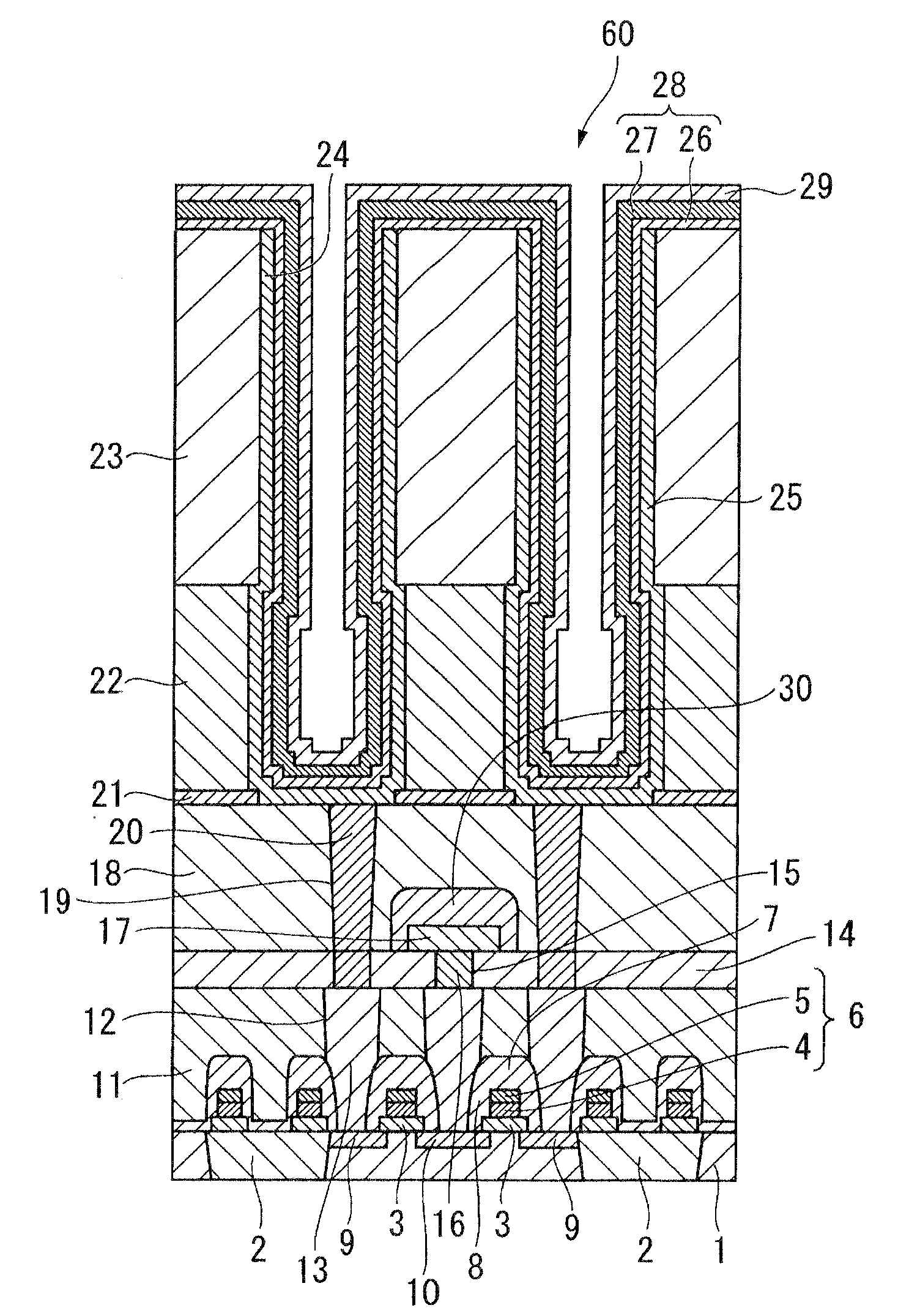
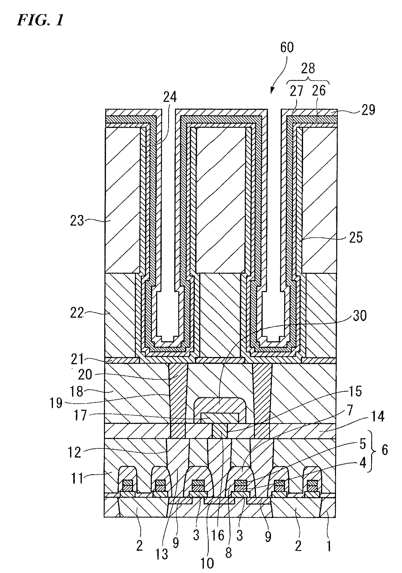
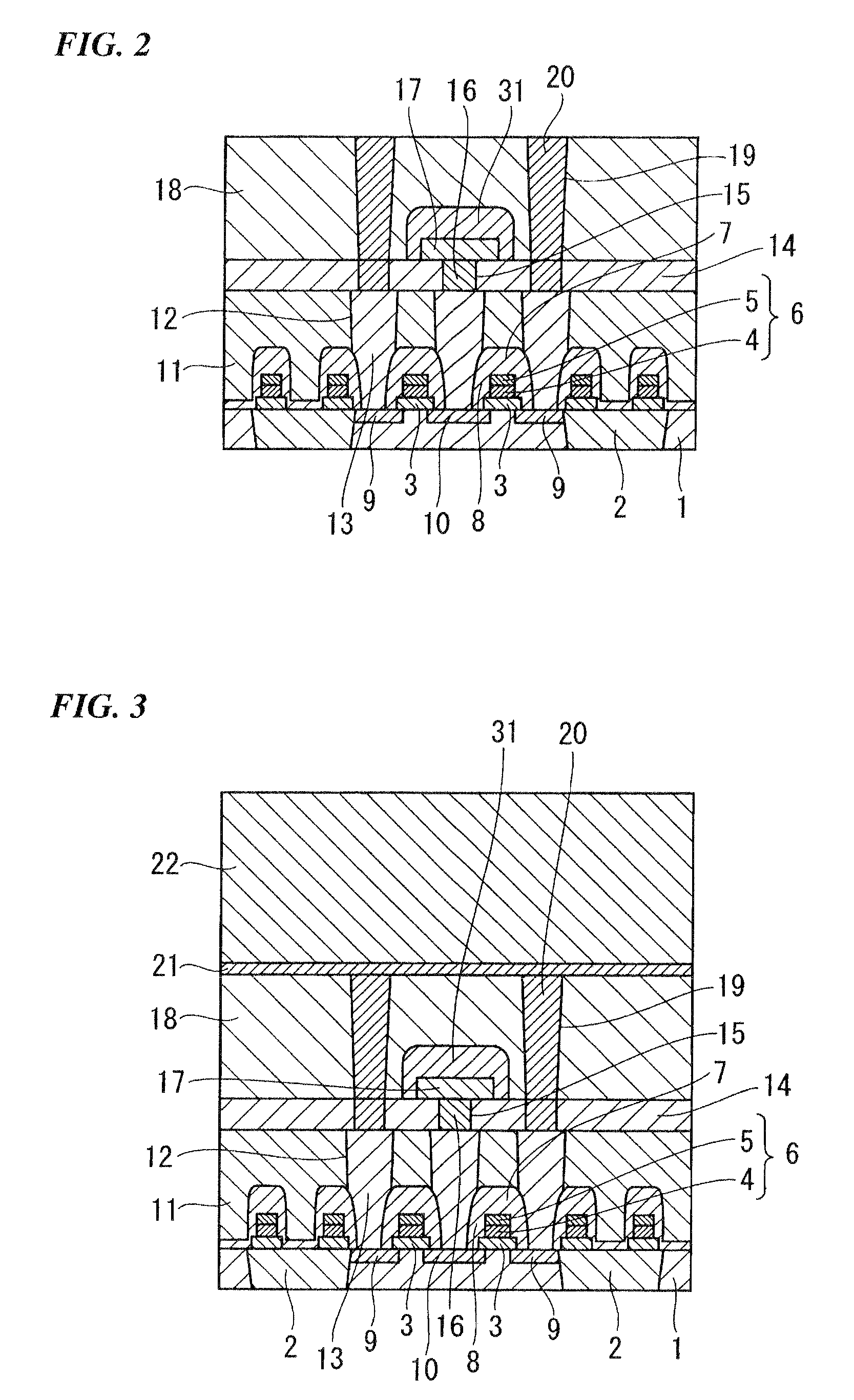
BACKGROUND OF THE INVENTION[0001]Priority is claimed on Japanese Patent Application No. 2006-355441, filed Dec. 28, 2006, the contents of which are incorporated herein by reference.FIELD OF THE INVENTION [0002]The present invention relates to a semiconductor device having a capacitor laminated in the form of a cylinder on a semiconductor substrate for use in a dynamic random access memory (DRAM), which is a so-called stacked capacitor, and a method of manufacturing the same.DESCRIPTION OF THE RELATED ART [0003]A capacitor structure of a DRAM (Dynamic Random Access Memory) includes an MIS (Metal Insulator Semiconductor) structure and an MIM (Metal Insulator Metal) structure (for example, see FIGS. 1 and 2 of Japanese Unexamined Patent Application, First Publication No. 2003-243534).[0004]In general, polycrystalline silicon doped with dopants is used for a semiconductor having the MIS structure. An example of an insulator in the MIS structure may include silicon oxide (SiO2), silicon ...

Claims


Application Information

Patent Timeline
Patent Type & Authority Applications(United States)
IPC IPC(8): H01L29/92H01L21/02
CPCH01L28/91H01L27/10852H10B12/033
Inventor HORIKAWA, MITSUHIRO
Owner PS4 LUXCO SARL
Learn More