Method of manufacturing liquid crystal display
- Summary
- Abstract
- Description
- Claims
- Application Information
AI Technical Summary
Benefits of technology
Problems solved by technology
Method used
Image
Examples
examples
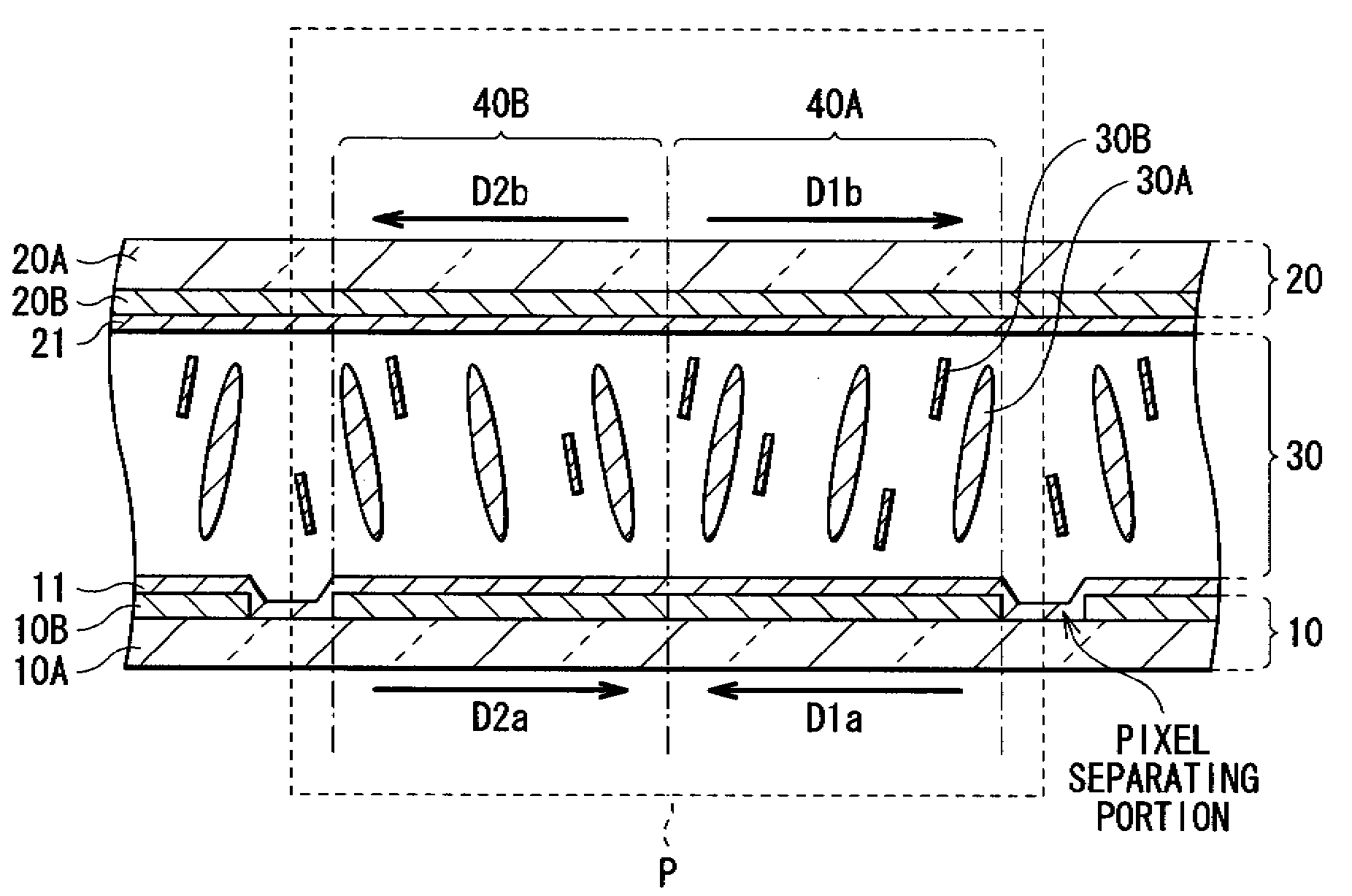
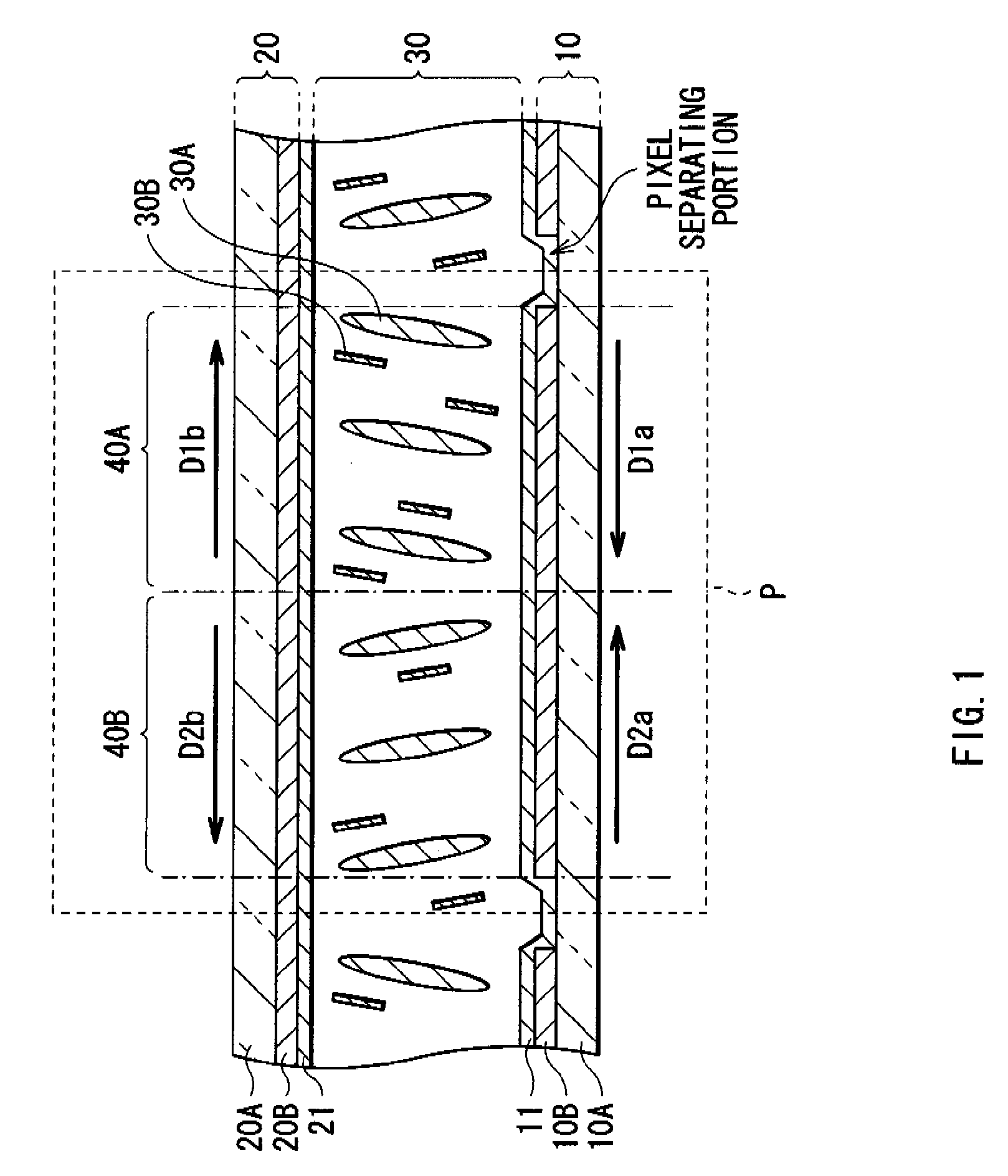
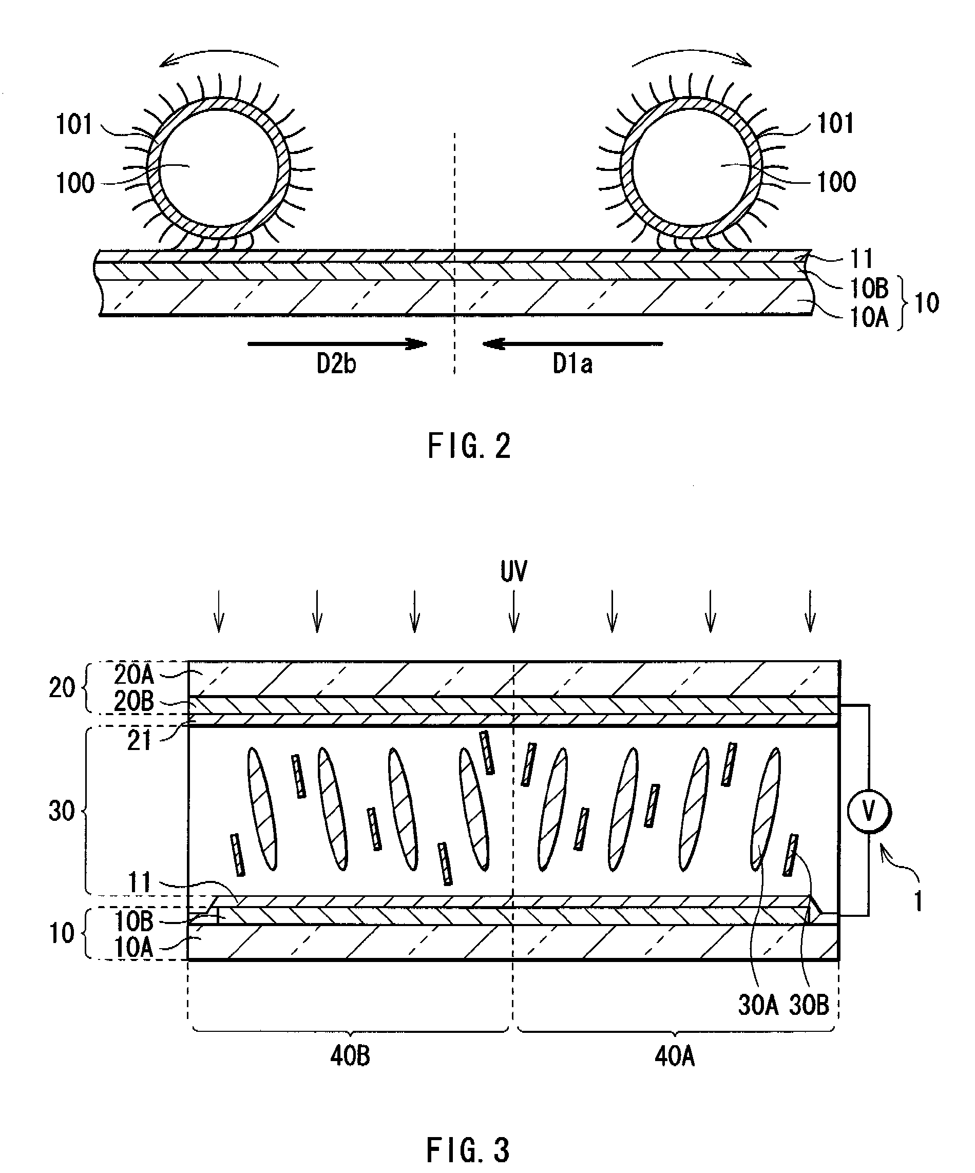
[0048]As an example, the following liquid crystal panel was manufactured in the following manner. Firstly, a vertical alignment film was applied to a TFT substrate, an array substrate having gate lines having a width of 15 μm, data lines having a width of 12 μm, a storage capacitor having a width of 20 μm, and pixel electrodes, and to a color filter substrate having a color filter, common electrodes and 4 μm-spacer projections. Subsequently, a rubbing process was performed to the respective substrates by using rolls with velvet wound thereon. Then, a resist material (for example, “TFR-970 PM 9CP,” manufactured by TOKYO OHKA KOGYO CO., LTD.) was applied to the respective substrates subjected to the rubbing processes, and the solvent was removed by high-temperature treatment. The substrates were then exposed through a mask having a predetermined pattern, and the uncured portions on the substrates were washed out with developer (for example, “NMD-3,” manufactured by TOKYO OHKA KOGYO CO...
PUM
| Property | Measurement | Unit |
|---|---|---|
| Magnetic field | aaaaa | aaaaa |
| Dielectric constant | aaaaa | aaaaa |
| Anisotropy | aaaaa | aaaaa |
Abstract
Description
Claims
Application Information
 - R&D
- Intellectual Property
- Life Sciences
- Materials
- Tech Scout
- Unparalleled Data Quality
- Higher Quality Content
- 60% Fewer Hallucinations
Browse by: Latest US Patents, China's latest patents, Technical Efficacy Thesaurus, Application Domain, Technology Topic, Popular Technical Reports.
© 2025 PatSnap. All rights reserved.Legal|Privacy policy|Modern Slavery Act Transparency Statement|Sitemap|About US| Contact US: help@patsnap.com


