Routing method for reducing coupling between wires of an electronic circuit
- Summary
- Abstract
- Description
- Claims
- Application Information
AI Technical Summary
Benefits of technology
Problems solved by technology
Method used
Image

Examples
Embodiment Construction
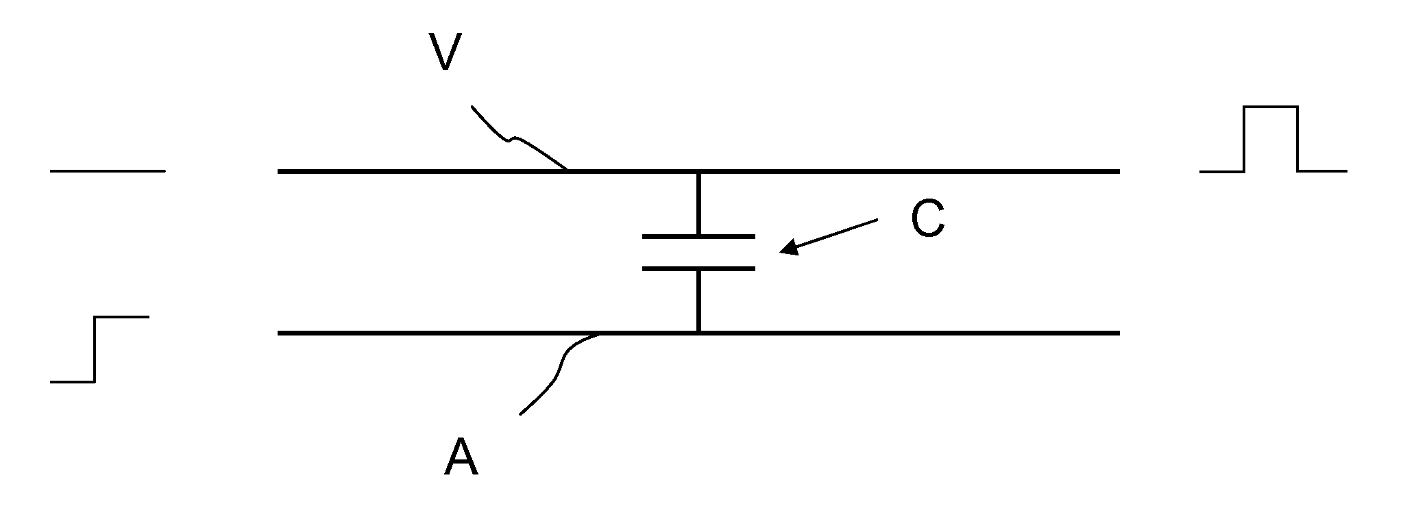
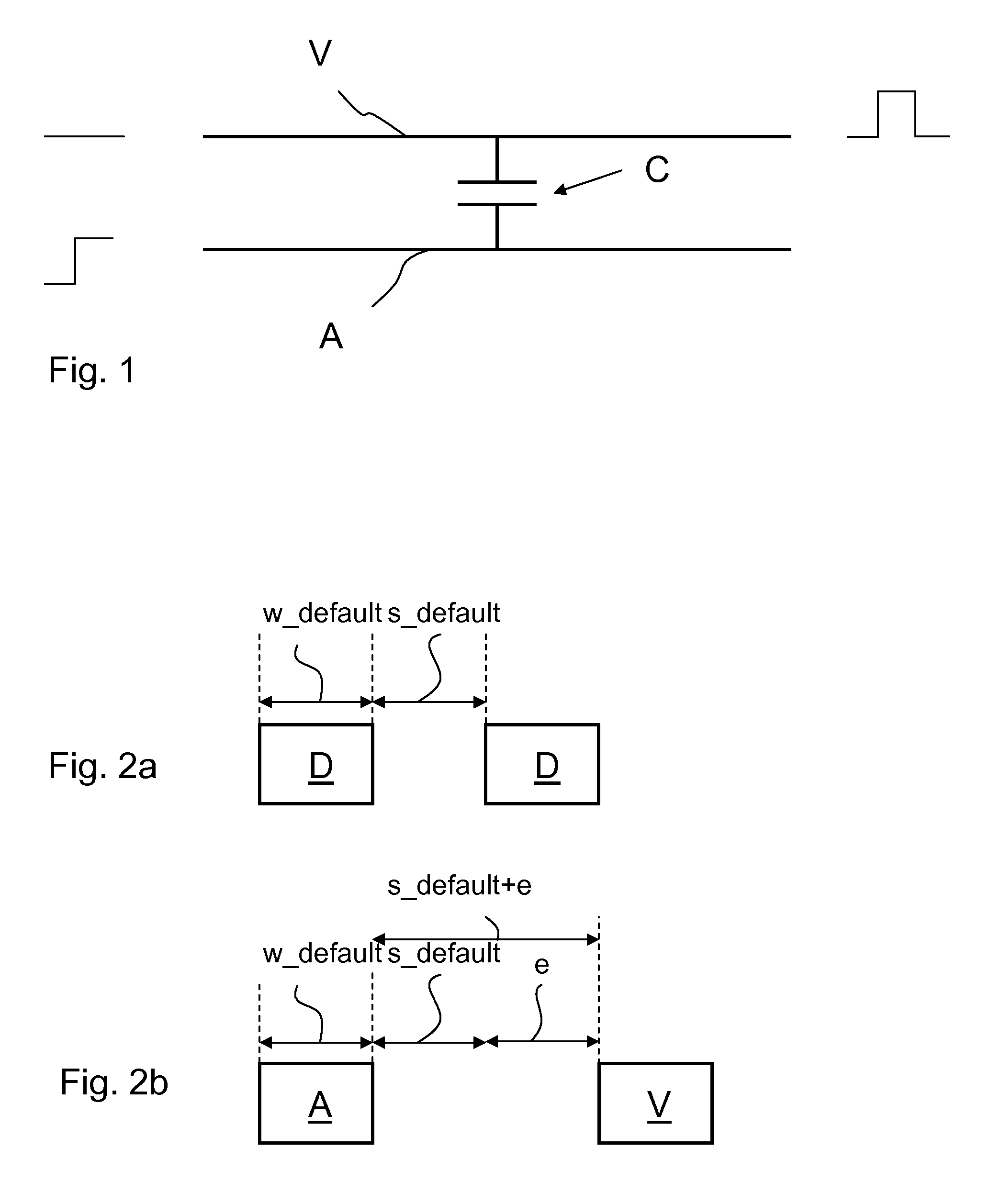
[0058]FIG. 1 schematically depicts a coupling issue between an aggressor wire A and a victim wire V. A capacitive coupling issue between the two wires A and V is indicated by a capacitor C.
[0059]A step like signal is applied to the aggressor wire A as indicated on the left side of the figure. The signal couples into the victim wire V yielding a pulse signal which falsifies the state of the victim wire V.
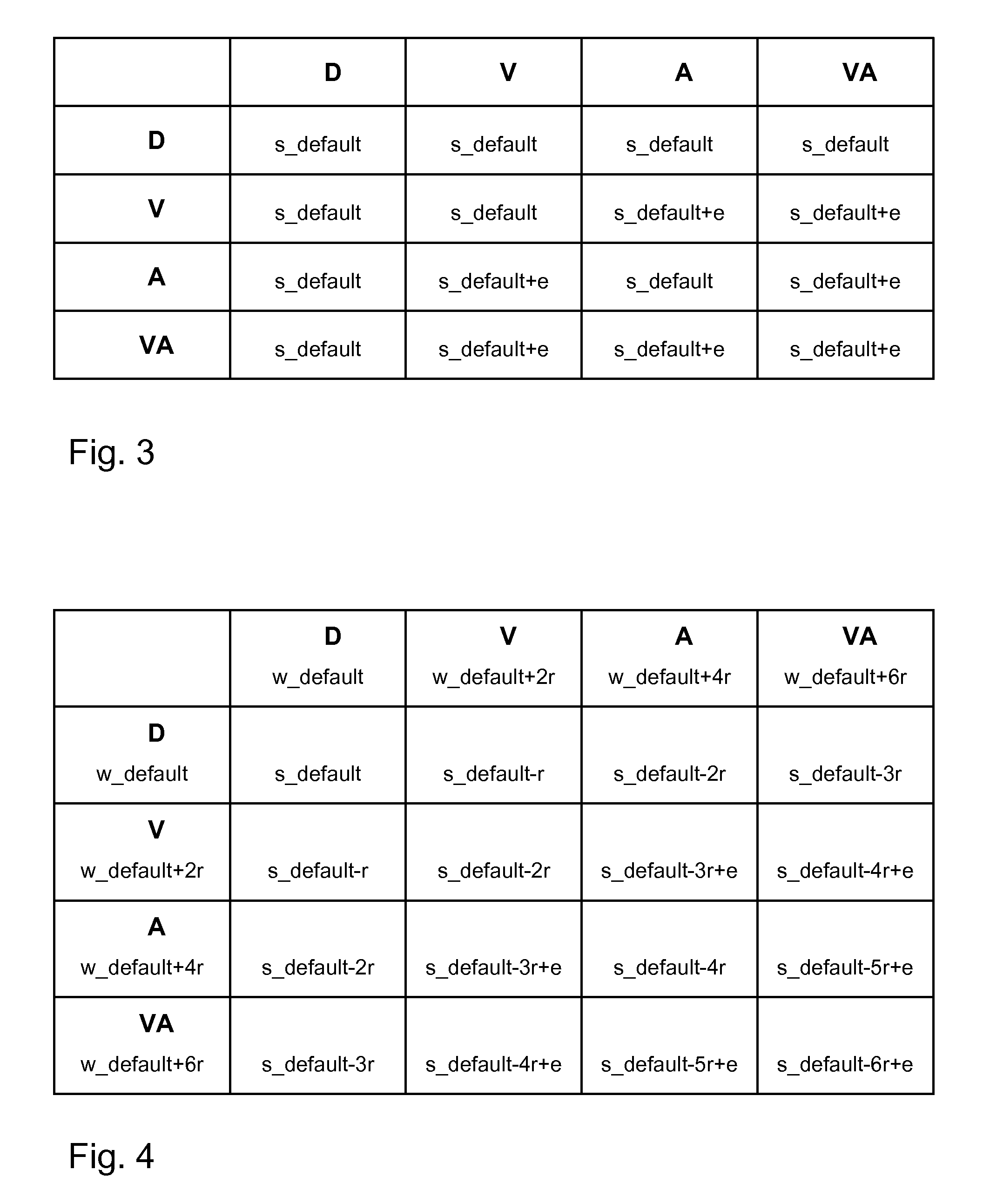
[0060]As depicted in the FIGS. 2a and 2b, a default wire D is assigned a default width w_default and a default spacing s_default to a proximate default wire D (FIG. 2a). The width and the spacing typically are a result of the actual technology files applied for a certain electronic circuit under development. As known in the art, those technology files typically comprise requirements for minimum wire widths, minimum spacings and other parameters which may be influenced by deposition and / or etching techniques, mask design, the specific layer of the wiring etc., which are applied in the...
PUM
 Abstract
Description
Claims
Application Information
 - Generate Ideas
- Intellectual Property
- Life Sciences
- Materials
- Tech Scout
- Unparalleled Data Quality
- Higher Quality Content
- 60% Fewer Hallucinations
Browse by: Latest US Patents, China's latest patents, Technical Efficacy Thesaurus, Application Domain, Technology Topic, Popular Technical Reports.
© 2025 PatSnap. All rights reserved.Legal|Privacy policy|Modern Slavery Act Transparency Statement|Sitemap|About US| Contact US: help@patsnap.com