
Composition and organic insulator prepared using the same

Active Publication Date: 2008-05-15
SAMSUNG ELECTRONICS CO LTD
View PDF10 Cites 4 Cited by
  • Summary
  • Abstract
  • Description
  • Claims
  • Application Information

AI Technical Summary

Benefits of technology

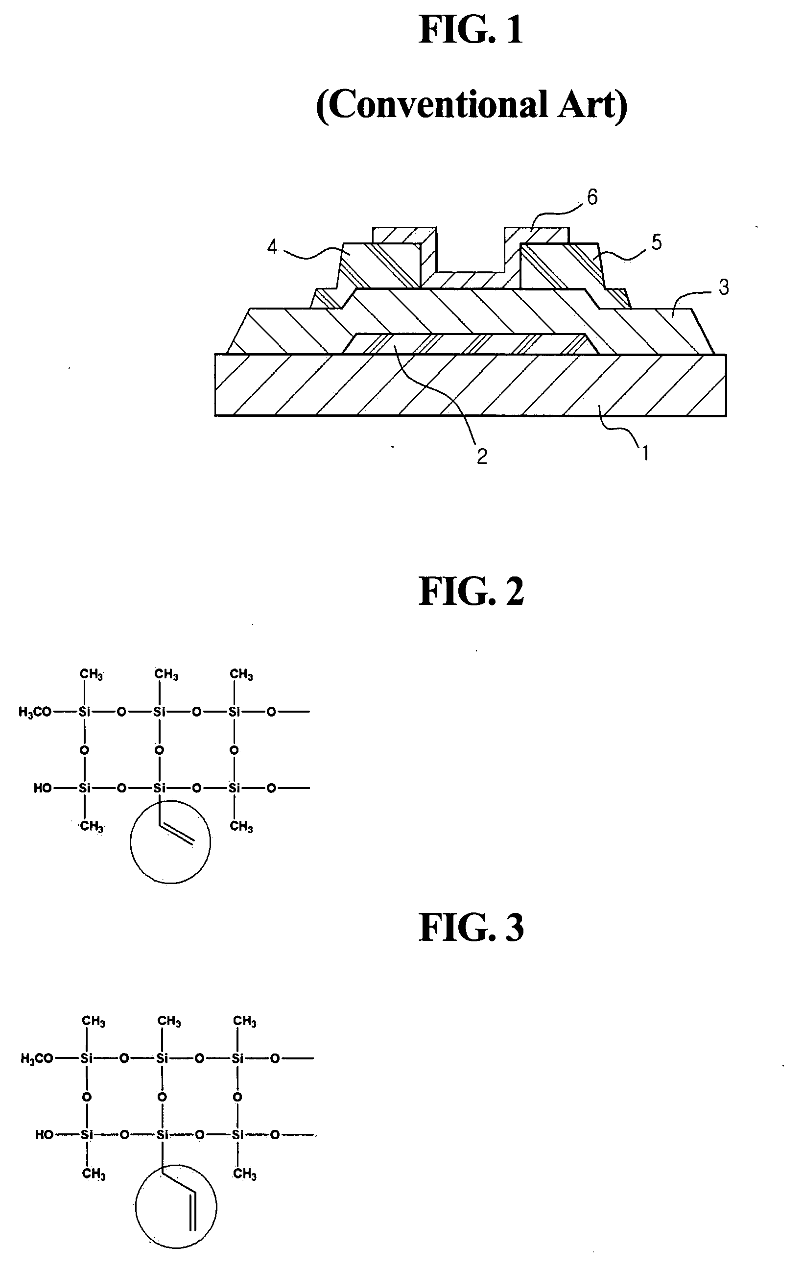
[0011]Accordingly, example embodiments have been made keeping in mind the above problems occurring in the related art, and example embodiments provide a composition for preparing an organic insulator, which has an increased crosslinking property in order to prepare an organic insulator th

Problems solved by technology

However, an operating voltage of about 100 V or more and a sub threshold voltage about 50 times higher than in the case of amorphous silicon are undesirably required.
), the use of various substrates may be restricted, and applying a printing process may be difficult.
Although an organic insulating film using polyimide, BCB (BenzoCycloButene) or photoacryl has been proposed, the device properties exhibited may not be desirable to the extent of substituting for inorganic insulating films.
However, the above method is undesirable because the ceramic particles negatively affect the formation of the organic active layer, and thus charge mobility may be decreased, and also leakage current may be increased, undesirably causing problems in which the above material should be provided in the form of a double structure along with an organic material having improved insulating properties.
However, a conventional crosslinking agent, mainly used for crosslinking the silane resins, may function to form a chemical bond between Si—OH groups or to chemically bind to Si—OH, and limitations may be thus imposed on increasing the crosslinking property.

Method used


Image

  • Composition and organic insulator prepared using the same
  • Composition and organic insulator prepared using the same
  • Composition and organic insulator prepared using the same

Examples


example 1

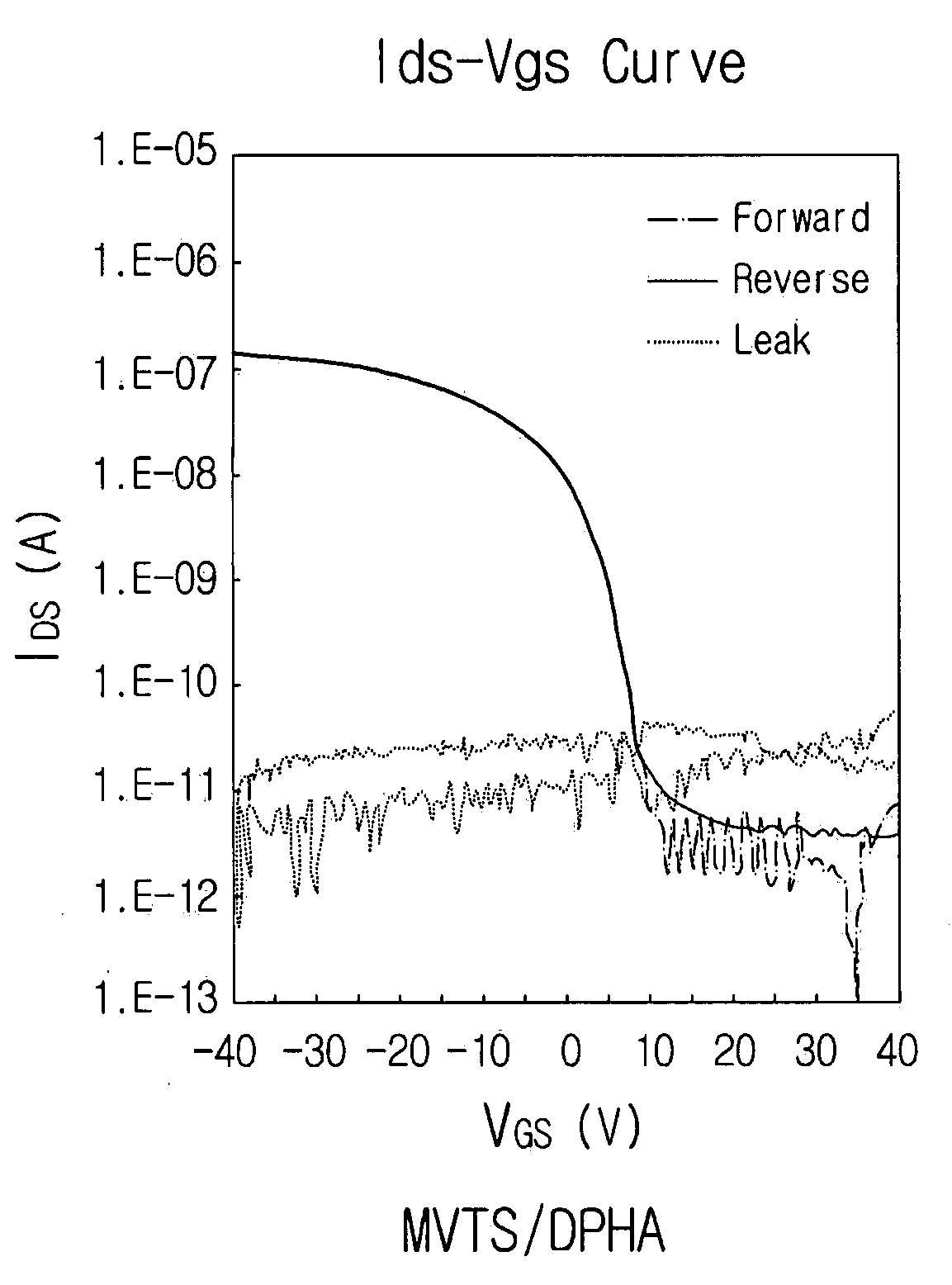
[0051]About 0.2 g of the MVTS obtained in Preparative Example 1 and about 0.04 g of a crosslinking agent, dipentaerythritol penta- / hexa-acrylate (DPHA), were added to about 1 g of n-butanol and then mixed well, thus preparing a mixture for an organic insulator. On an Al / Nd gate pattern on a glass substrate, the mixture for an organic insulator was applied through spin coating to thus form a film, which was then subjected to pre-annealing at about 70° C. for about 2 min, UV irradiation (about 500 mJ / cm2), and then baking at about 200° C. for about 1 hour, thereby forming an insulating layer. On the insulating layer thus formed, about 1 wt % polythiophene in chloroform was applied to a thickness of about 1000 Å through spin coating at about 2000 rpm, therefore forming a semiconductor layer. On the above active layer, source / drain electrodes were formed using gold (Au) metal through a top contact process with the use of a shadow mask having a channel length of about 100 μm and a channe...

example 2

[0052]An OTFT was manufactured in the same manner as in Example 1, with the exception that about 0.2 g of the PVTS obtained in Preparative Example 2 was used, instead of about 0.2 g of the MVTS.

example 3

[0053]An OTFT was manufactured in the same manner as in Example 1, with the exception that about 0.2 g of the MATS obtained in Preparative Example 3 was used, instead of about 0.2 g of the MVTS.


PUM

PropertyMeasurementUnit
Percent by massaaaaaaaaaa
Angleaaaaaaaaaa
Compositionaaaaaaaaaa

Abstract

Disclosed is a composition for preparing an organic insulator, including an organic silane material, having a vinyl group, an acetylene group or an acryl group as a functional group for participating in a crosslinking reaction, a crosslinking agent, and a solvent for dissolving the above components. The organic insulator of example embodiments may be provided in the form of a solid insulating film, which may increase charge mobility while decreasing the threshold voltage and operating voltage of OTFTs, and which also may generate relatively slight hysteresis.

Description

PRIORITY STATEMENT[0001]This non-provisional application claims priority under U.S.C. § 119(a) to Korean Patent Application No. 2006-111601, filed on Nov. 13, 2006, in the Korean Intellectual Property Office (KIPO), the entire contents of which are incorporated herein by reference.BACKGROUND[0002]1. Field[0003]Example embodiments relate to a composition for preparing an organic insulator having a crosslinking property, an organic insulator prepared using the same, an organic thin film transistor (OTFT) including the organic insulator, an electronic device including the OTFT and methods of fabricating the same. Other example embodiments relate to a composition for preparing an organic insulator, comprising an organic silane material, a crosslinking agent, and a solvent, an organic insulator prepared using the same, an organic thin film transistor (OTFT) including the organic insulator, an electronic device including the OTFT and methods of fabricating the same.[0004]2. Description of...

Claims


Application Information

Patent Timeline
IPC IPC(8): H01L51/30B05D3/06B05D5/12H01L51/40C08F30/08
CPCC08F283/12C08F290/068C08G77/12C08G77/24H01L51/0545C08L83/04C08L83/06H01L51/0036H01L51/052C08K5/10H10K85/113H10K10/471H10K10/466C08L83/02C08L101/02
Inventor JEONG, EUN JEONGKIM, JOO YOUNGSON, KYUNG SEOKLEE, EUN KYUNGLEE, SANG YOON
Owner SAMSUNG ELECTRONICS CO LTD
Learn More