Component-embedded board fabrication method and apparatus for high-precision and easy fabrication of component-embedded board with electronic components embedded in wiring board

Active Publication Date: 2008-05-15
SHINKO ELECTRIC IND CO LTD
View PDF8 Cites 0 Cited by
  • Summary
  • Abstract
  • Description
  • Claims
  • Application Information

AI Technical Summary

Benefits of technology

[0037] According to the present invention, when fabricating a component-embedded board, if an electronic component formed on the board is displaced from the design position thereof, the design data to be used in the subsequent processing of the board is corrected by taking the displacement into account, and the wiring pattern formation and the via formation using the maskless exposure or inkjet technology are performed based on the corrected design data; as a result, the component-embedded board can be fabricated easily, even if the electronic component is somewhat displaced in position, and the fabrication yield improves drastically compared with the prior art that uses a photomask.
[0038] Furthermore, the present invention can easily cope with a situation where, during the trial production of the component-embedded board, for example, an urgent change has to be made to the circuit configuration without changing the design drawing itself.

Problems solved by technology

One possible way to avoid such a positional displacement would be to form the electronic component as faithfully to the design data as possible, but it would be extremely costly to implement such a high-precision fabrication process.
Furthermore, once the board with the electronic component formed thereon is covered with an insulating layer, it is difficult to locate the position of the electronic component.
Accordingly, even if a displacement or distortion is caused in the formation of the electronic component, the subsequent processes have to be performed in accordance with the design data, eventually ending up in the production of a defective part.
As described, in the prior art, it is difficult to locate the position of the electronic component once it is covered with an insulating layer; as a result, with increasing number of layers in the board and with increasing miniaturization of the wiring pattern, it becomes increasingly difficult to fabricate a defect-free circuit board.

Method used


Image

  • Component-embedded board fabrication method and apparatus for high-precision and easy fabrication of component-embedded board with electronic components embedded in wiring board
  • Component-embedded board fabrication method and apparatus for high-precision and easy fabrication of component-embedded board with electronic components embedded in wiring board
  • Component-embedded board fabrication method and apparatus for high-precision and easy fabrication of component-embedded board with electronic components embedded in wiring board

Examples


first embodiment

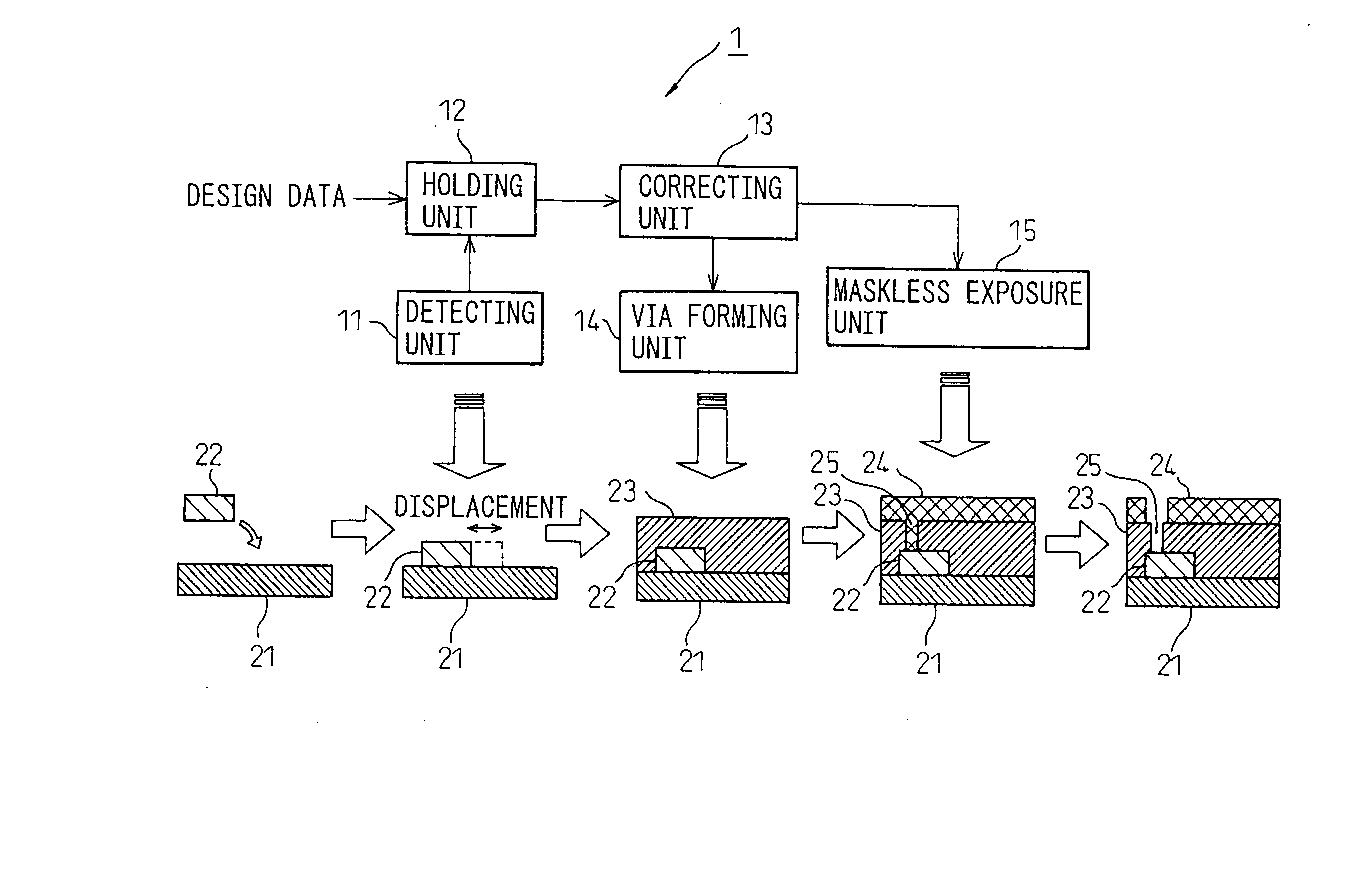
[0060] First, a description will be given of the present invention applied to the fabrication of a multilayered component-embedded board.

[0061]FIGS. 6a to 11b are diagrams for explaining the first embodiment of the component-embedded board fabrication method according to the present invention.

[0062] First, as shown in FIG. 6a, an electronic component 22-1 is formed by positioning it in accordance with design data on the surface of a board 21 which is not yet covered with an insulating layer.

[0063] The board used here is, for example, a glass epoxy board, and the electronic component is, for example, a semiconductor device, a capacitor, a resistor, or the like. In the example shown in FIG. 6a, the electronic component 22-1 is mounted and formed as a discrete component on the bare board surface, but a passive component (electronic component) such as an inductor, capacitor, or resistor may be formed by fabricating it in integral fashion using a thin-film process such as sputtering or...

second embodiment

[0094] Next, a description will be given of the present invention applied to the fabrication of a multilayered component-embedded board.

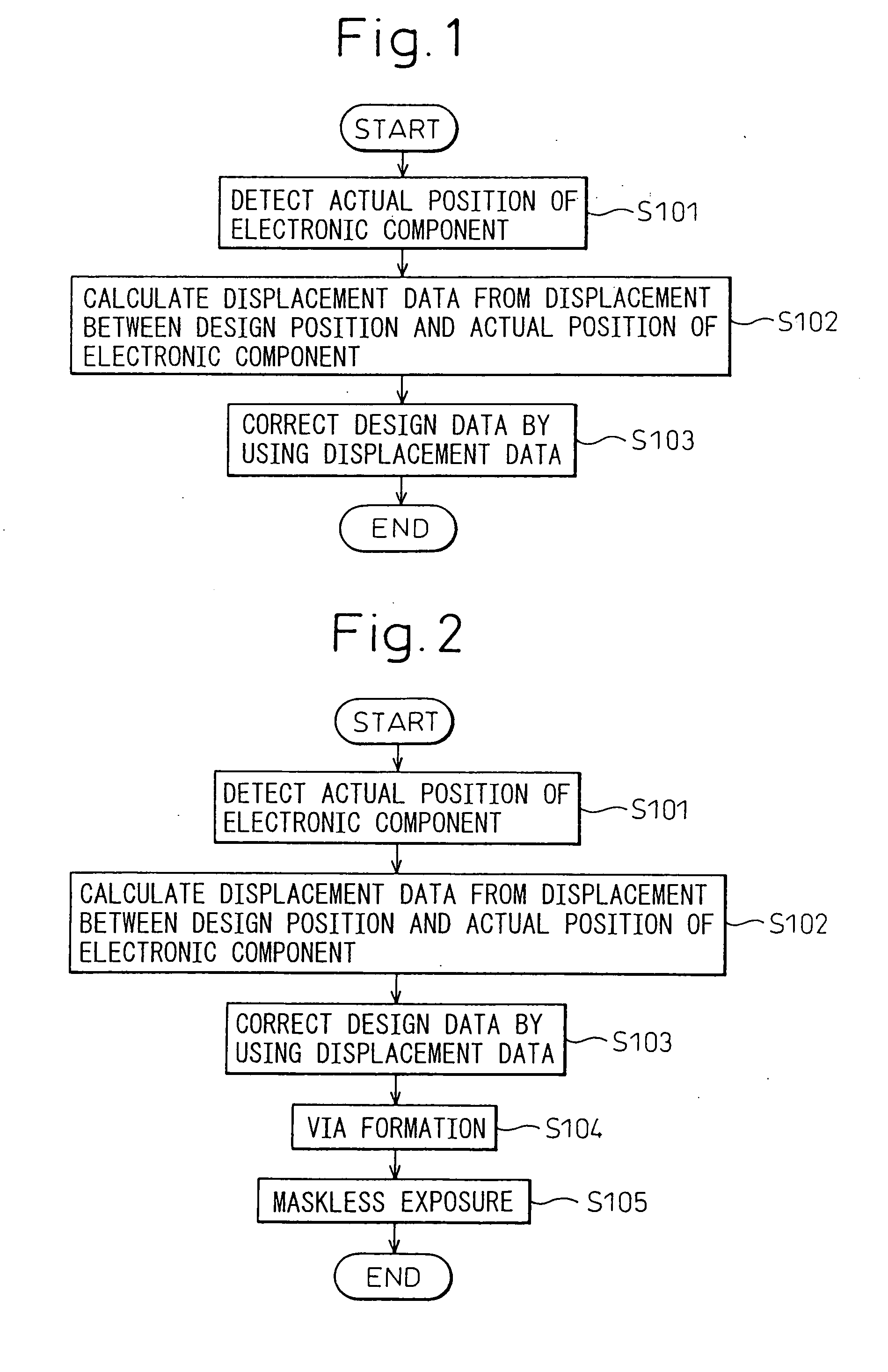
[0095] As already explained with reference to FIG. 6b, according to the present invention, the displacement data indicating the displacement between the design position of the electronic component 22-1 and the actual position of the electronic component 22-1 formed on the surface of the board 21 is calculated and stored in advance. In the first embodiment of the invention described above, the design data necessary when performing the maskless exposure is dynamically corrected using the displacement data.

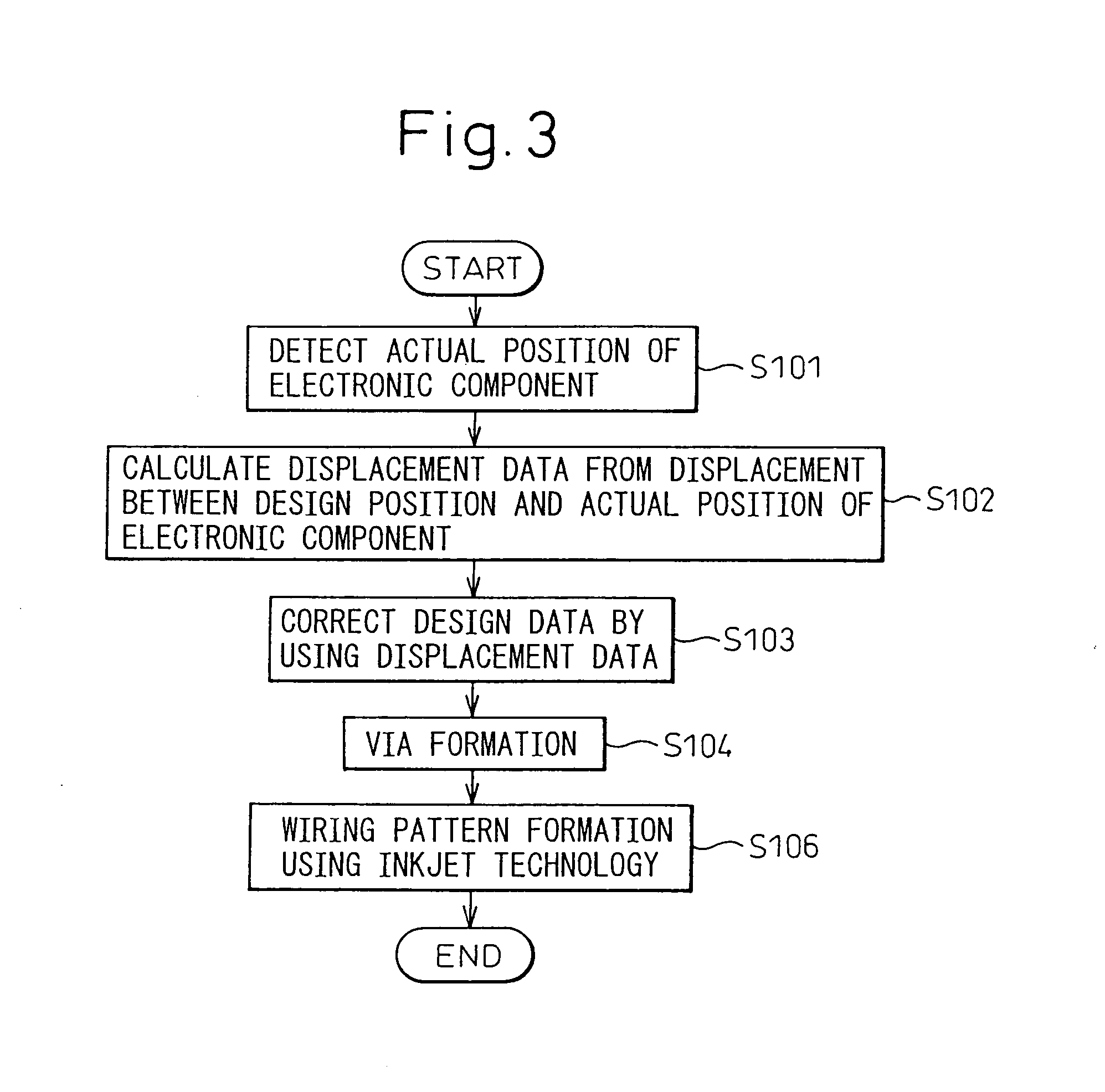
[0096] On the other hand, in the second embodiment of the invention, the wiring pattern is directly formed (patterned) by using inkjet technology, not the maskless exposure. Design data necessary for the direct patterning is dynamically corrected using the displacement data in the same manner as previously described. That is, the wiring pattern form...


PUM

PropertyMeasurementUnit
Displacementaaaaaaaaaa

Abstract

An apparatus 1 for fabricating a component-embedded board according to the present invention comprises: a detecting unit 11 for detecting, before the board 21 is covered with an insulating layer 23, the actual position of an electronic component 22 formed on the surface of the board 21; a holding unit 12 for calculating a displacement between the design position of the electronic component 22 and the actual position of the electronic component 22 on the surface of the board 21, and for holding the displacement as displacement data; and a correcting unit 13 for correcting, based on the displacement data, design data to be used for processing the board 21 after the board 21 is covered with the insulating layer 23.

Description

CROSS-REFERENCE TO RELATED APPLICATION [0001] This application is a divisional of U.S. application Ser. No. 10 / 612,222, filed Jul. 3, 2003 and claims priority to Japanese Applications No. 2002-200055 and 2002-352440, which are incorporated by reference herein in their entireties.BACKGROUND OF THE INVENTION [0002] 1. Field of the Invention [0003] The present invention relates to a component-embedded board fabrication method for fabricating a component-embedded board with electronic components embedded in a wiring board, and an apparatus using the same. [0004] 2. Description of the Related Art [0005] With the increasing miniaturization and complexity of wiring patterns formed on printed circuit boards, a need is increasing for high-precision wiring forming technologies. On the other hand, as electronic apparatuses shrink in size and increase in performance, multilayered wiring boards are increasingly used. In some wiring boards (hereinafter called “component-embedded boards”), various...

Claims


Application Information

Patent Timeline
IPC IPC(8): H01K3/10G06F19/00H05K3/46H01L21/60H01L23/538H05K1/18
CPCH01L23/5389Y10T29/49117H01L24/82H01L24/97H01L2224/24011H01L2224/2402H01L2224/24226H01L2224/76155H01L2224/97H01L2924/01003H01L2924/01004H01L2924/01013H01L2924/01015H01L2924/01029H01L2924/01033H01L2924/01038H01L2924/01039H01L2924/01056H01L2924/01073H01L2924/01078H01L2924/14H01L2924/19041H01L2924/19042H01L2924/19043H01L2924/30105H01L2924/30107H05K1/185H01L24/24Y10T29/49165Y10T29/49004Y10T29/53087Y10T29/49155Y10T29/49146H01L2924/01005H01L2924/01006H01L2924/01024H01L2224/32225H01L2224/73267H01L2224/92244H01L2224/8203H01L2224/82102Y10T29/53174Y10T29/532Y10T29/53061Y10T29/49126Y10T29/49131H01L2224/82H01L2924/00H01L2924/12042H05K3/46
Inventor AKAGAWA, MASATOSHISEKIGAWA, KAZUNARIWAKABAYASHI, SHINICHI
Owner SHINKO ELECTRIC IND CO LTD
Why Eureka
Try Eureka