
Modifiable gate stack memory element

Inactive Publication Date: 2008-05-01
RISING SILICON
View PDF18 Cites 41 Cited by
  • Summary
  • Abstract
  • Description
  • Claims
  • Application Information

AI Technical Summary

Benefits of technology

[0006]An embodiment of the invention provides a memory cell design and method for storing information, including using an integrated circuit including a transistor having a source, a drain, a channel, a gate oxid...

Problems solved by technology

A key challenge for flash memory and other non-volatile memory technologies over the next few years is achieving the densities that are increasingly required by the market.
This requires that the cell size be continually reduced, which introduces a variety of challenges in design and manufacturing.

Method used


Image

  • Modifiable gate stack memory element
  • Modifiable gate stack memory element
  • Modifiable gate stack memory element

Examples


Embodiment Construction

[0023]Mass production of memory products, such as DRAM and NAND flash memory, with 50 nm node technology will soon be the industry norm. As memory technologies are scaled down to a 50 nm or smaller node size, it is expected that they will encounter a variety of technical issues that cannot be addressed by simply scaling existing technologies. Instead, new approaches will be needed, including new device structures, new process technologies, and new materials.

[0024]For DRAM, key design features include a storage capacitor and low leakage current at the storage node connected to the capacitor. The refresh interval, which is a key parameter describing DRAM performance, is governed by the stored charge loss at the capacitor. The leakage current at the storage node includes leakage through the capacitor itself, junction leakage current at the storage node, and sub-threshold conduction from a cell transistor. As the design rule shrinks down, the capacitance of the storage capacitor decreas...


PUM


Abstract

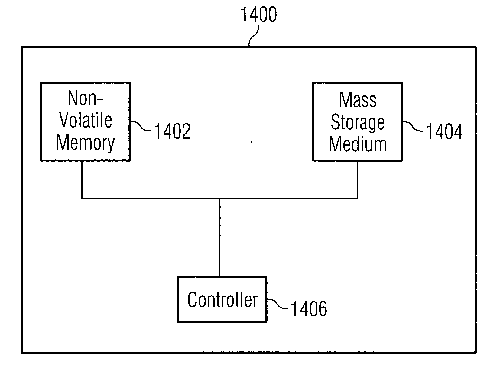
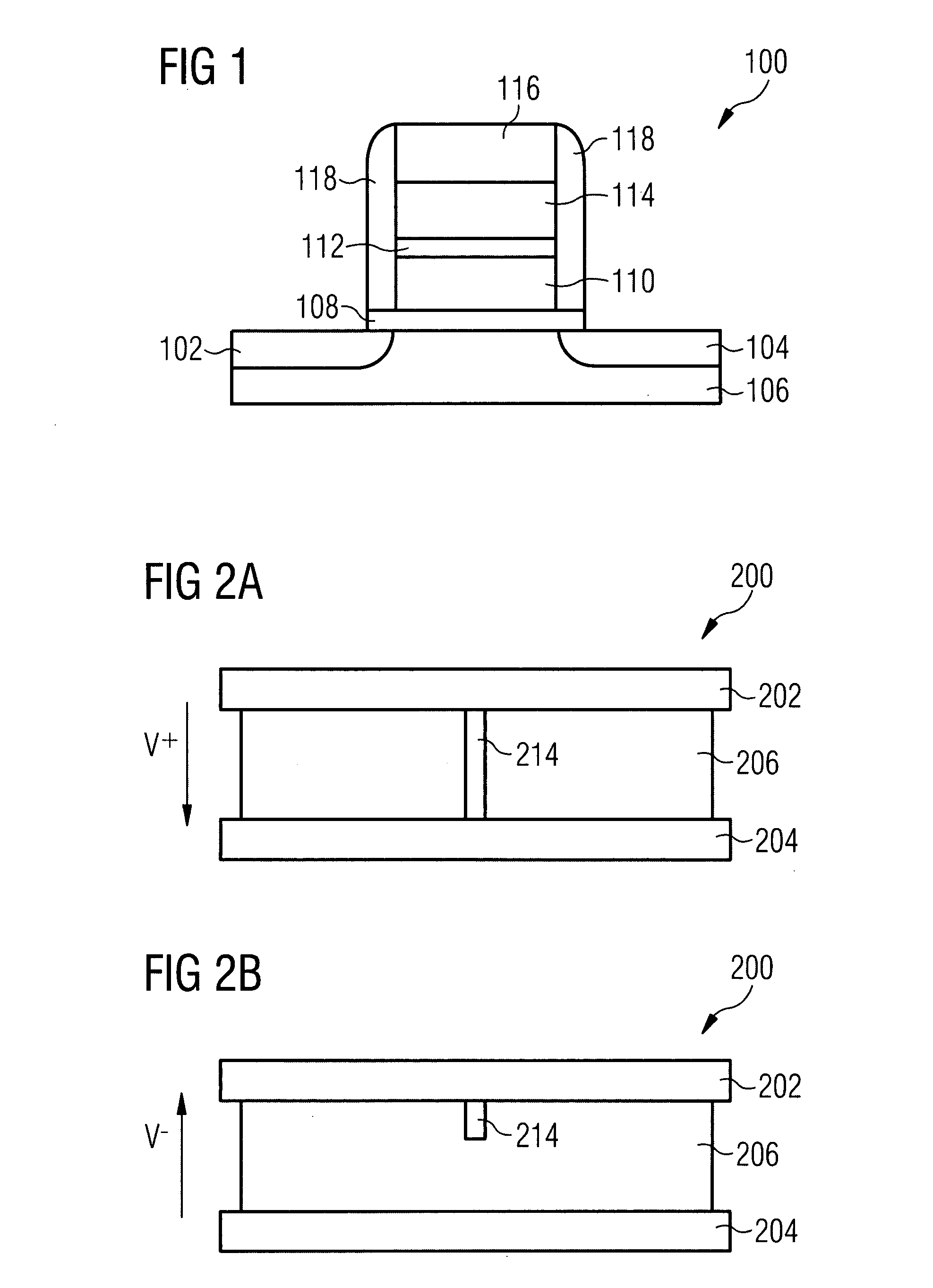
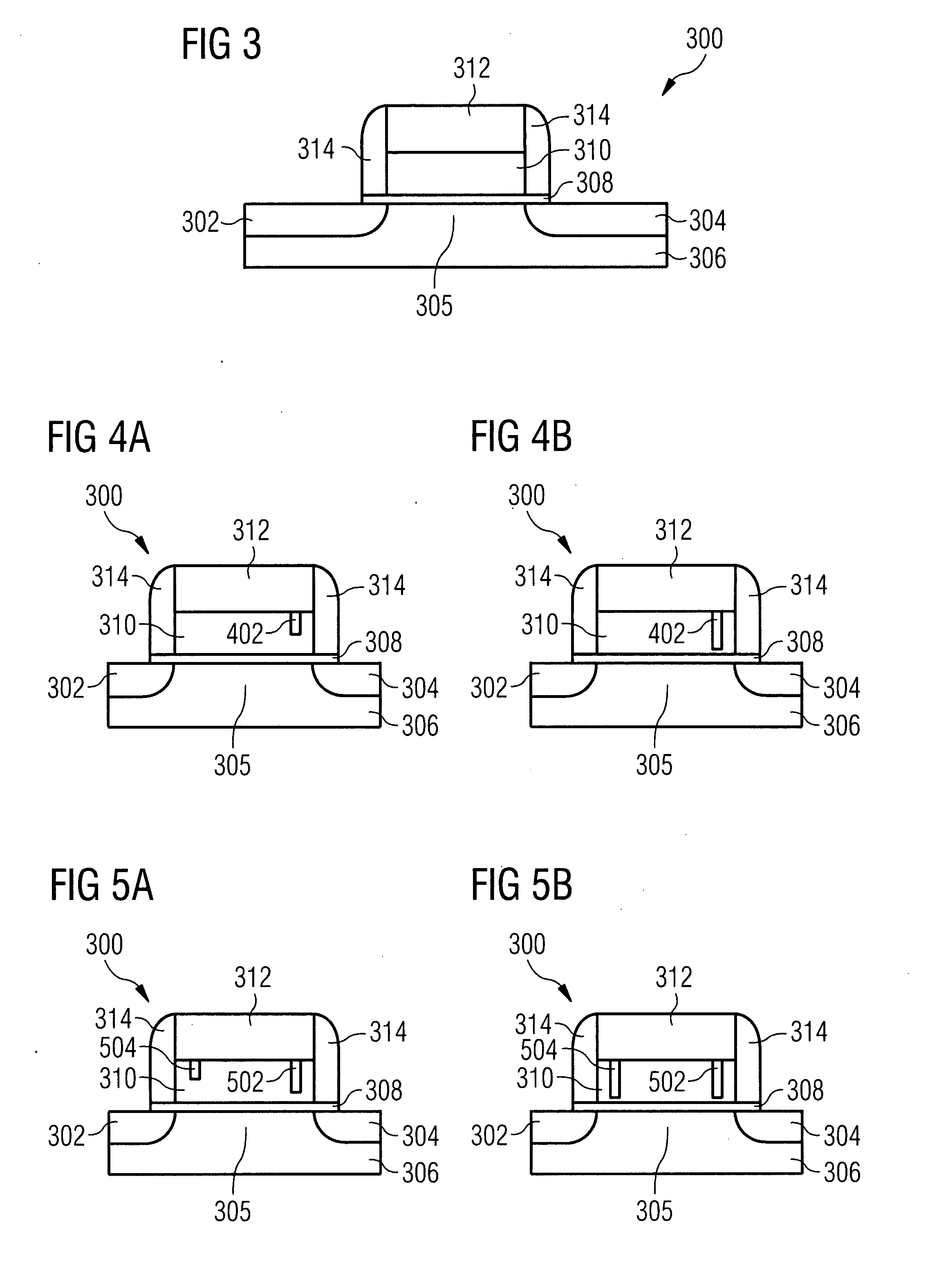
An apparatus and method for storing information are provided, including using an integrated circuit including a transistor having a channel, a gate oxide layer, a gate electrode, and a modifiable gate stack layer. To store information, the on-resistance of the transistor is changed by causing a non-charge-storage based physical change in the modifiable gate stack layer.

Description

CROSS-REFERENCES TO RELATED APPLICATIONS[0001]This application is a continuation-in-part of U.S. patent application Ser. No. 11 / 588,865, entitled “Modifiable Gate Stack Memory Element,” filed Oct. 27, 2006.TECHNICAL FIELD[0002]The present invention relates generally to a memory and in one embodiment to a modifiable gate stack memory element.BACKGROUND[0003]Non-volatile memory, such as flash memory, retains its stored data even when power is not present. One common type of non-volatile memory is flash memory, which is used in a wide variety of electronic equipment, including digital cameras, portable audio players, wireless communication devices, personal digital assistants, peripheral devices, and for storing firmware in computers and other devices.[0004]A key challenge for flash memory and other non-volatile memory technologies over the next few years is achieving the densities that are increasingly required by the market. This requires that the cell size be continually reduced, wh...

Claims


Application Information

Patent Timeline
IPC IPC(8): G11C16/10H01L21/336H01L29/788
CPCG11C13/0004H01L29/7887G11C13/0011G11C2213/31G11C2213/32G11C2213/53G11C2213/71H01L29/0673H01L29/42324H01L29/42368H01L29/42376H01L29/513H01L29/517H01L29/66825H01L29/66833H01L29/78H01L29/7881G11C13/0007
Inventor KREUPL, FRANZ
Owner RISING SILICON
Learn More