
Circuitized substrate with internal resistor, method of making said circuitized substrate, and electrical assembly utilizing said circuitized substrate

Inactive Publication Date: 2008-04-17
TTM TECH NORTH AMERICA LLC +1
View PDF31 Cites 29 Cited by
  • Summary
  • Abstract
  • Description
  • Claims
  • Application Information

AI Technical Summary

Benefits of technology

[0050] It is, therefore, a primary object of the present invention to enhance the circuitized substrate art by providing a circuitized substrate having the advantageous features taught herein.
[0051] It is another object of the invention to provide a method of making such a circuitized substrate which can be accomplished in a relatively facile manner and at relatively low costs.
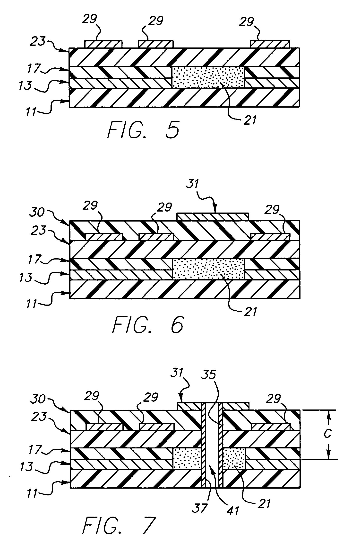
[0054] According to one aspect of the invention, there is provided a method of making a circuitized substrate having circuitry including a resistor as part thereof the method comprising the steps of providing a first dielectric layer, forming a first electrical conductor on the first dielectric layer, forming an opening within the first electrical conductor, positioning a quantity of resistor material within the opening, forming a second dielectric layer substantially over the quantity of resistor material within the opening, forming a second electrical conductor on the second dielectric layer, and forming an electrical connection between the second and first electrical conductors, the quantity of resistor material serving to substantially reduce the capacitance between the electrical conductors and increase the high frequency resistance in the electrical connection between the electrical conductors.
[0055] According to another aspect of the invention, there is provided a circuitized substrate comprising a first dielectric layer, a first electrical conductor positioned on the first dielectric layer and including an opening therein, a quantity of resistor material within the opening, a second dielectric layer positioned substantially over the quantity of resistor material, a second electrical conductor positioned on the second dielectric layer, and an electrical connection between the second and first electrical conductors, the quantity of resistor material serving to substantially reduce the capacitance between the first and second electrical conductors and increase the high frequency resistance in the electrical connection between the first and second electrical conductors.
[0056] According to yet another aspect of the invention, there is provided an electrical assembly comprising a circuitized substrate including a first dielectric layer, a first electrical conductor positioned on the first dielectric layer and including an opening therein, a quantity of resistor material within the opening, a second dielectric layer positioned substantially over the quantity of resistor material, a second electrical conductor positioned on the second dielectric layer, and an electrical connection between the second and first electrical conductors, the quantity of resistor material serving to substantially reduce the capacitance between the first and second electrical conductors and increase the high frequency resistance in the electrical connection between the first and second electrical conductors, and at least one electrical component positioned on and electrically coupled to the circuitized substrate.

Problems solved by technology

The discrete passive devices occupy a relatively high percentage of the surface area of the completed substrate, which is undesirable from a future design aspect because of the increased need and demand for miniaturization in today's substrates and products containing same art.
Use of pre-fired and ground ceramic nano-powders in the dielectric layer poses obstacles for the formation of thru-holes (conductive holes permitting electronic communication between conductive layers of a PCB), however.
The distribution within the dielectric layer of particles of different size often presents major obstacles to thru-hole formation where the thru-holes are of extremely small diameter, also referred to in the industry as micro-vias due to the presence of the larger particles.
Another problem associated with pre-fired ceramic nano-powders is the ability for the dielectric layer to withstand substantial voltage without breakdown occurring across the layer.
This is even further undesirable because, as indicated by the equation cited above, greater planar capacitance may also be achieved by reducing the thickness of the dielectric layer.
That is, the resulting PCB still requires the utilization of external devices thereon, and thus does not afford the PCB external surface area real estate savings mentioned above which are desired and demanded in today's technology.
Although the pre-fired and ground dielectric formulations produced by solid phase reactions are acceptable for many electrical applications, these suffer from several disadvantages.
First, the milling step may serve as a source of contaminants, which can adversely affect electrical properties.
Consequently, films produced using these powders are limited to thicknesses greater than the size of the largest particle.
Thirdly, powder suspensions or composites produced using pre-fired ground ceramic powders must be used immediately after dispersion, due to the high sedimentation rates associated with large particles.
It is thus clear that methods of making PCBs which rely on the advantageous features of using nano-powders as part of the PCB's internal components or the like, such as those described in selected ones of the above patents, possess various undesirable aspects which are detrimental to providing a PCB with optimal functioning capabilities when it comes to internal resistance, capacitance or other electrical properties.
As is known, extremely close positioning of such thru-holes and signal lines may result in discontinuities occurring therein, which will adversely affect the successful operation of the product, especially at high frequencies (which are also demanded in many products today).

Method used


Image

  • Circuitized substrate with internal resistor, method of making said circuitized substrate, and electrical assembly utilizing said circuitized substrate
  • Circuitized substrate with internal resistor, method of making said circuitized substrate, and electrical assembly utilizing said circuitized substrate
  • Circuitized substrate with internal resistor, method of making said circuitized substrate, and electrical assembly utilizing said circuitized substrate

Examples


example one

[0087] Fifty grams (gm) of cycloaliphatic epoxy resin (e.g., one sold under product designation “ERL-4211” by the Union Carbide Corporation, Danbury, Conn.) was mixed with about 50 gm of hexahydro-4-methylphthalic anhydride and 0.4 gm N,N dimethyl benzylamine. The mixed solution was stirred for approximately ten minutes to assure uniform mixing. Fifty gm of silver powder available from Degussa Corporation (having a business location at 379 Interpace Parkway, Parsippany, N.J.) was added to 7.5 gm of the mixed solution and formed into a printable paste. The silver powder included particles with an average size of about five microns. A layer of this paste material was then printed onto a copper substrate. This layer was then cured at approximately 190 degrees Celsius (C) for about two hours. The resistance of the cured resistors (3 inch long and 0.003 square inch cross section area) measured about 120 milliohms (mΩ).

example two

[0088] Fifty gm of the “ERL-4211” cycloaliphatic epoxy resin was mixed with about fifty gm of hexahydro-4-methylphthalic anhydride and 0.4 gm N,N dimethyl benzylamine. The mixed solution was stirred for about ten minutes to assure uniform mixing. Fifty gm of copper powder was added to 7.5 gm of the mixed solution and formed into a printable paste. The copper powder included particles with an average size of about four microns. A layer of this paste material was printed onto a copper substrate. This layer was then cured at approximately 190° C. for about two hours. The resistance of the cured resistors (3 inch long and 0.003 square inch cross section area) measured about 120 Mega ohms (MΩ).

example three

[0089] Fifty gm of the “ERL-4211” cycloaliphatic epoxy resin was mixed with about fifty gm of hexahydro-4-methylphthalic anhydride and 0.4 gm N,N dimethyl benzylamine. The mixed solution was stirred for about ten minutes to assure uniform mixing. Thirty-eight gm of copper and twelve gm of silver powder was added to 7.5 gm of the mixed solution and formed into a printable paste. The average particle sizes for the copper and silver powders ranged from about four to about five microns in diameter. A layer of this paste material was printed onto a copper substrate. This layer was then cured at approximately 190° C. for about two hours. The resistance of the cured resistors (3 inch long and 0.003 square inch cross section area) measured about 70 Mega ohms (MΩ).


PUM

PropertyMeasurementUnit
Dielectric polarization enthalpyaaaaaaaaaa
Electrical resistanceaaaaaaaaaa
Electrical conductoraaaaaaaaaa

Abstract

A circuitized substrate which utilizes at least one internal (embedded) resistor as part thereof, the resistor comprised of a material including resin and a quantity of powders of nano-particle and / or micro-particle sizes. The resistor serves to decrease the capacitance in the formed circuit while only slightly increasing the high frequency resistance, thereby improving circuit performance through the substantial elimination of some discontinuities known to exist in structures like these. An electrical assembly (substrate and at least one electrical component) is also provided.

Description

TECHNICAL FIELD [0001] The present invention relates to providing resistors within circuitized substrates such as printed circuit boards, chip carriers and the like, and more specifically to a method for doing so and to products including such internal resistors as part thereof. Even more particularly, the invention relates to such methodologies and products wherein the internal resistors are formed using powder materials having nano-particles or micro-particles or combinations of both as part thereof. CROSS REFERENCE TO CO-PENDING APPLICATIONS [0002] In Ser. No. ______, filed Apr. 6, 2007 under Attorney's docket number EI-2-06-013, end entitled “Non-Flaking Capacitor Material, Capacitive Substrate Having An Internal Capacitor Therein Including Said Non-Flaking Capacitor Material And Method Of Making A Capacitor Member For Use In A Capacitive Substrate,” there is defined a capacitor material including a thermosetting resin (e.g., epoxy resin), a high molecular mass flexibilizer (e.g...

Claims


Application Information

Patent Timeline
IPC IPC(8): H05K1/16H05K3/10
CPCH05K1/095H05K1/116Y10T29/49165H05K3/429H05K2203/0568H05K1/167
Inventor DAS, RABINDRA N.ROWLANDS, MICHAEL J.
Owner TTM TECH NORTH AMERICA LLC
Learn More