Multi-valued data recording spin injection maganetization reversal element and device using the element
a multi-valued data and maganetization reversal technology, applied in the field of multi-valued data recording spin injection maganetization reversal element and the use of a device, can solve the problems of large element resistance, large electric power consumption for writing information in magnetic field production by means of current, and insufficient for high-density recording and regeneration, etc., to achieve large electric resistance, increase the electric resistance of the element, and increase the thickness
- Summary
- Abstract
- Description
- Claims
- Application Information
AI Technical Summary
Benefits of technology
Problems solved by technology
Method used
Image

Examples
example 1
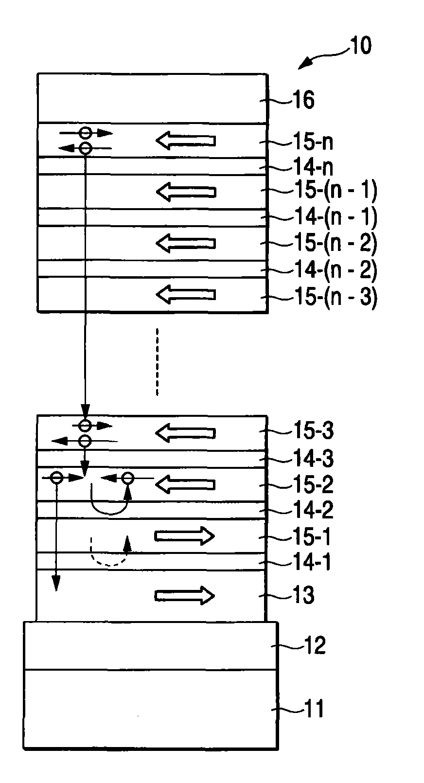
[0080]By using the arrangement shown in FIG. 1, a GMR magnetic memory element was made in which two layers of ferromagnetic layers were provided and nonmagnetic metal was used for the isolation layers.
[0081]For nonmagnetic substrate 11, a Si substrate was used. On the Si substrate, a Cu film was deposited to a thickness of 200 nm as fixed layer electrode 12 with a shape of 1 μm in width and 10 μm in length. Subsequent to this, on fixed layer electrode 12, ferromagnetic fixed layer 13 was formed by using Co70Cr20Pt10 to a thickness of 100 nm with a shape of 500 nm in width and 1 μm in length. (Here, subscript numerals represent atomic percentages. The same applies to the following.) Following this, the following layers were formed with the same length and width as those of ferromagnetic fixed layer 13. Namely, first isolation layer 14-1 of Cu with a thickness of 1 nm, first ferromagnetic free layer 15-1 of Co89Pt10Cr1 with a thickness of 10 nm, second isolation layer 14-2 of Cu with ...
example 2
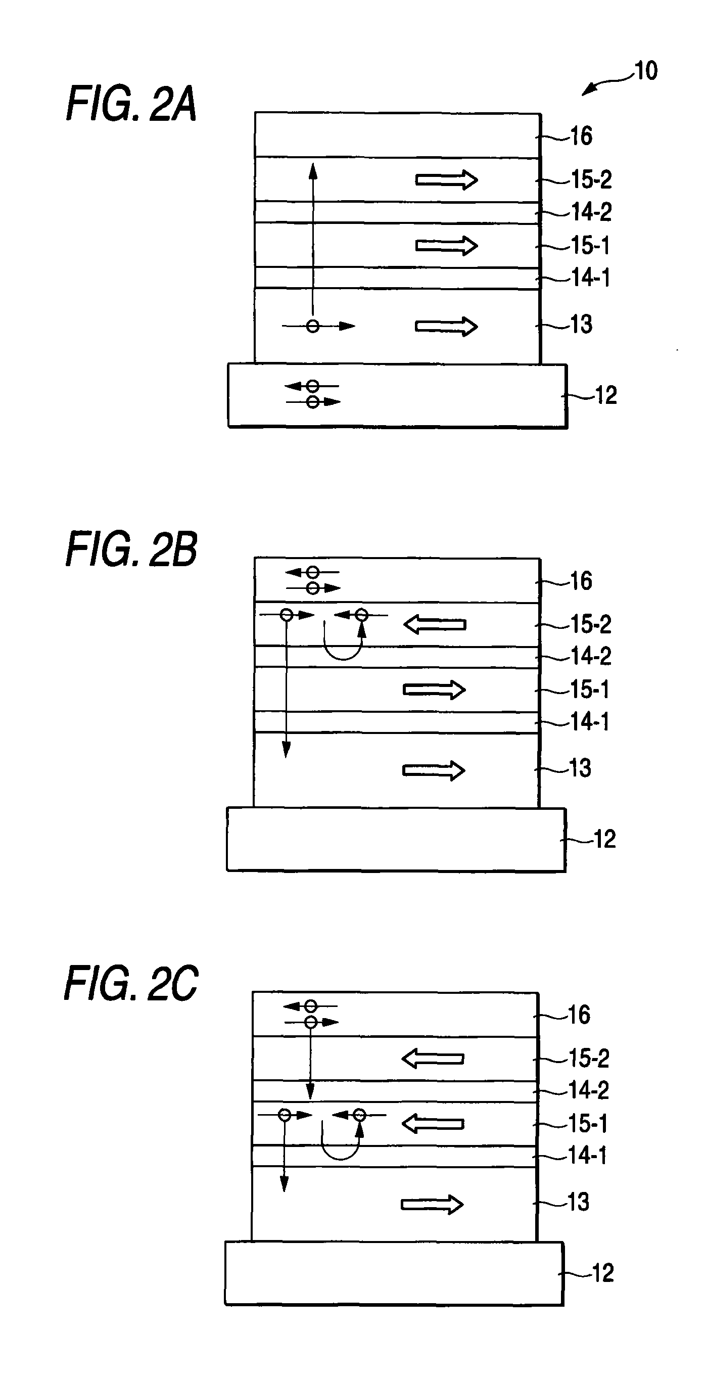
[0082]This is an example of making a TMR magnetic memory element. A magnetic memory element having the TMR effect was obtained in quite the same way as that in Example 1 except that an Al2O3 layer with a thickness of 1 nm was formed by sputtering as each of the first and second isolation layers 14-1 and 14-2.
[0083]By using the element in Example 2, three-valued data recording was carried out. First, Ku and Ic of each of the ferromagnetic free layers were measured, by which it was confirmed that Ku1 and Ic1 in the first ferromagnetic free layer were 4.0×10⁶ erg / cm3 and 1.0×10⁸ A / cm2, respectively, Ku2 and Ic2 in the second ferromagnetic free layer were 3.3×10⁶ erg / cm3 and 5.0×10⁷ A / cm2, respectively, and Ku1>Ku2 and Ic1>IC2.
[0084]Next, three-valued data were recorded and read out according to the operation modes shown in Table 1. The results of the reading out are shown in Table 2. The current densities for writing are 1.2×10⁸ A / cm2 for the logical value “0”, 6.0×10⁷ A / cm2 for the lo...
PUM
| Property | Measurement | Unit |
|---|---|---|
| current | aaaaa | aaaaa |
| current | aaaaa | aaaaa |
| spin relaxation length | aaaaa | aaaaa |
Abstract
Description
Claims
Application Information
 - R&D
- Intellectual Property
- Life Sciences
- Materials
- Tech Scout
- Unparalleled Data Quality
- Higher Quality Content
- 60% Fewer Hallucinations
Browse by: Latest US Patents, China's latest patents, Technical Efficacy Thesaurus, Application Domain, Technology Topic, Popular Technical Reports.
© 2025 PatSnap. All rights reserved.Legal|Privacy policy|Modern Slavery Act Transparency Statement|Sitemap|About US| Contact US: help@patsnap.com