ESD protection for bipolar-CMOS-DMOS integrated circuit devices and modular method of forming the same

a technology of integrated circuit devices and protection, which is applied in the direction of semiconductor devices, semiconductor/solid-state device details, electrical apparatus, etc., can solve the problems of reducing the efficiency of esd energy distribution, affecting the complete isolation of the device by the fabrication of the p-type substrate material, and affecting the complete isolation of the device by the cmos

Inactive Publication Date: 2008-02-07
ADVANCED ANALOGIC TECHNOLOGIES INCORPORATED +1
View PDF7 Cites 49 Cited by
  • Summary
  • Abstract
  • Description
  • Claims
  • Application Information

AI Technical Summary

Problems solved by technology

ESD devices with higher trigger voltages generally rely on a lateral breakdown mechanism that is prone to current crowding, making it difficult to design large structures that effectively distribute the ESD energy.
Fabrication of conventional CMOS in P-type substrate material does not facilitate complete isolation of its devices since every P-type well forming the body (back-gate) of NMOS transistors is shorted to the substrate potential, typically the most negat...

Method used


Image

  • ESD protection for bipolar-CMOS-DMOS integrated circuit devices and modular method of forming the same
  • ESD protection for bipolar-CMOS-DMOS integrated circuit devices and modular method of forming the same
  • ESD protection for bipolar-CMOS-DMOS integrated circuit devices and modular method of forming the same

Examples


Embodiment Construction

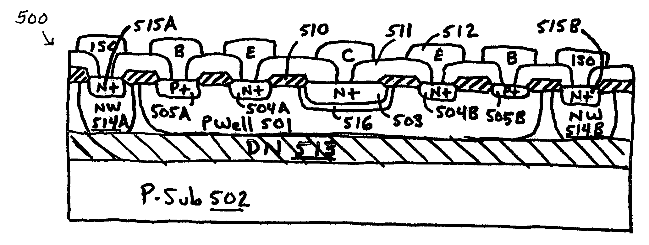
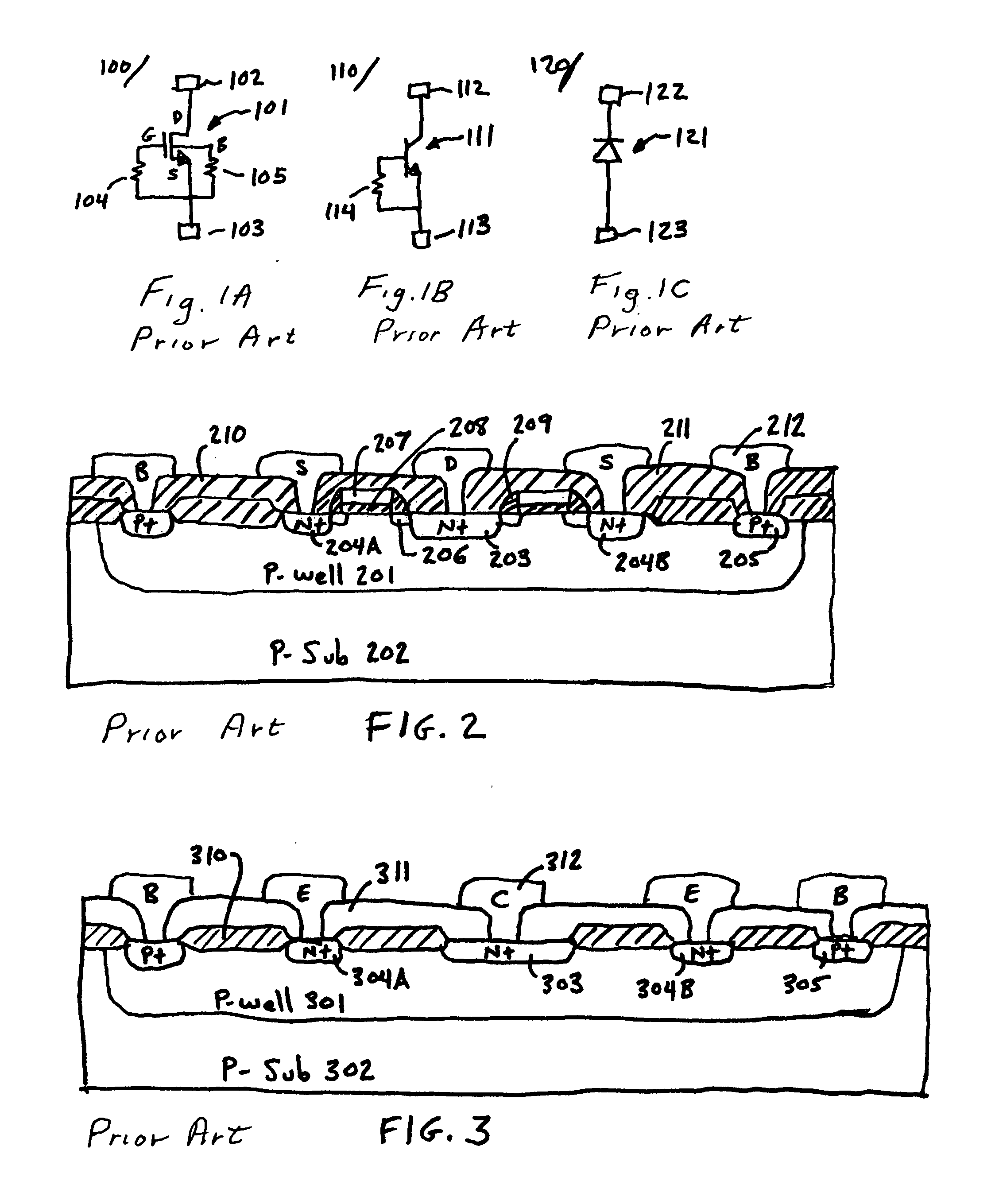
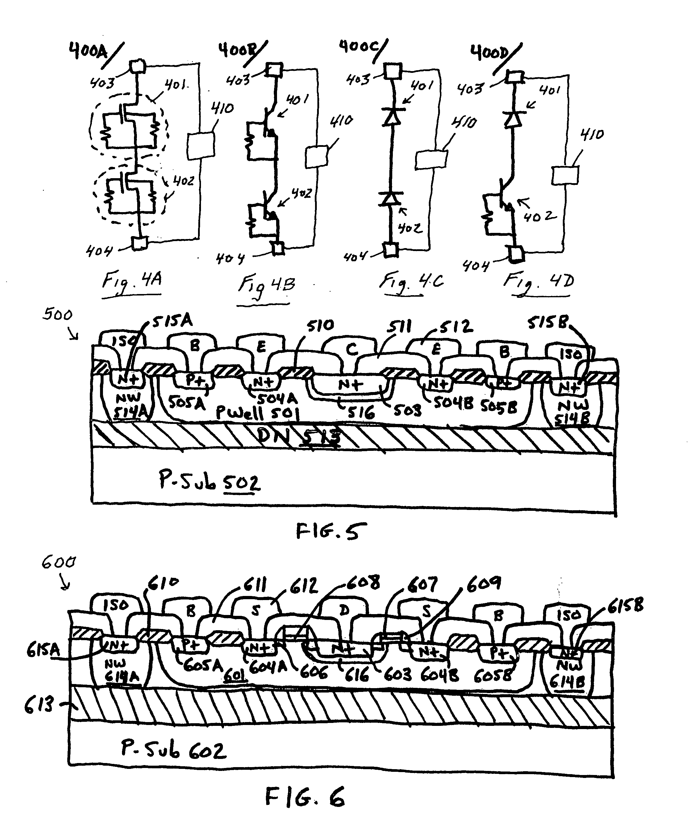
[0023]An all low-temperature fabrication method using as-implanted junction isolation structures employs high-energy and chain implants with dopant implanted through contoured oxides to achieve fully-isolated bipolar, CMOS and DMOS devices without the need for isolation diffusions, epitaxy or high temperature processes. The low-temperature wafer fabrication methods and isolated device structures were previously described in pending U.S. application Ser. No. 11 / 298,075 and in U.S. Pat. Nos. 6,855,985, 6,900,091 and 6,943,426 to R. K. Williams et al., each of which is incorporated herein by reference.

[0024]The inventive matter in this application is related to these patents and applications but concentrates on the design and integration of isolated and stackable ESD protection structures.

[0025]The low-temperature fabrication of the high-voltage devices described in this application are compatible with the modular low-temperature fabrication methods described in the aforementioned appl...


PUM


Abstract

An Electro-Static Discharge (ESD) protection device is formed in an isolated region of a semiconductor substrate. The ESD protection device may be in the form of a MOS or bipolar transistor or a diode. The isolation structure may include a deep implanted floor layer and one or more implanted wells that laterally surround the isolated region. The isolation structure and ESD protection devices are fabricated using a modular process that includes virtually no thermal processing. Since the ESD device is isolated, two or more ESD devices may be electrically “stacked” on one another such that the trigger voltages of the devices are added together to achieve a higher effective trigger voltage.

Description

FIELD OF THE INVENTION[0001]This invention relates to semiconductor chip fabrication and in particular to methods of fabricating and electrically isolating bipolar, CMOS and DMOS transistors and passive components in a semiconductor chip monolithically at high densities without the need for high temperature fabrication processing steps, and to provide ESD protection for such devices.BACKGROUND OF THE INVENTION[0002]In the fabrication of integrated circuit (IC) chips, it is frequently necessary to electrically isolate devices that are formed on the surface of the chip, especially when these components operate at different voltages. Such complete electrical isolation is necessary to integrate certain types of transistors including bipolar junction transistors and various metal-oxide-semiconductor (MOS) transistors including power DMOS transistors. Complete isolation is also needed to allow CMOS control circuitry to float to potentials well above the substrate potential during operatio...

Claims


Application Information

Patent Timeline
IPC IPC(8): H01L23/62
CPCH01L27/0251H01L29/0626H01L29/0692H01L29/866H01L29/735H01L29/7833H01L29/861H01L29/7317
Inventor DISNEY, DONALD RAYCHEN, JUN-WEIWILLIAMS, RICHARD K.RYU, HYUNGSIKCHAN, WAI TIEN
Owner ADVANCED ANALOGIC TECHNOLOGIES INCORPORATED
Why Eureka
Try Eureka