
Capacitive node isolation for electrostatic discharge circuit

Inactive Publication Date: 2008-01-31
ATMEL CORP
View PDF15 Cites 2 Cited by
  • Summary
  • Abstract
  • Description
  • Claims
  • Application Information

AI Technical Summary

Benefits of technology

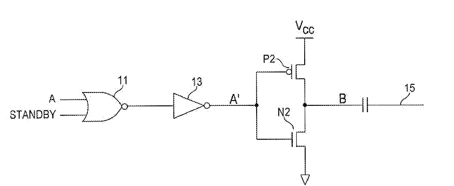
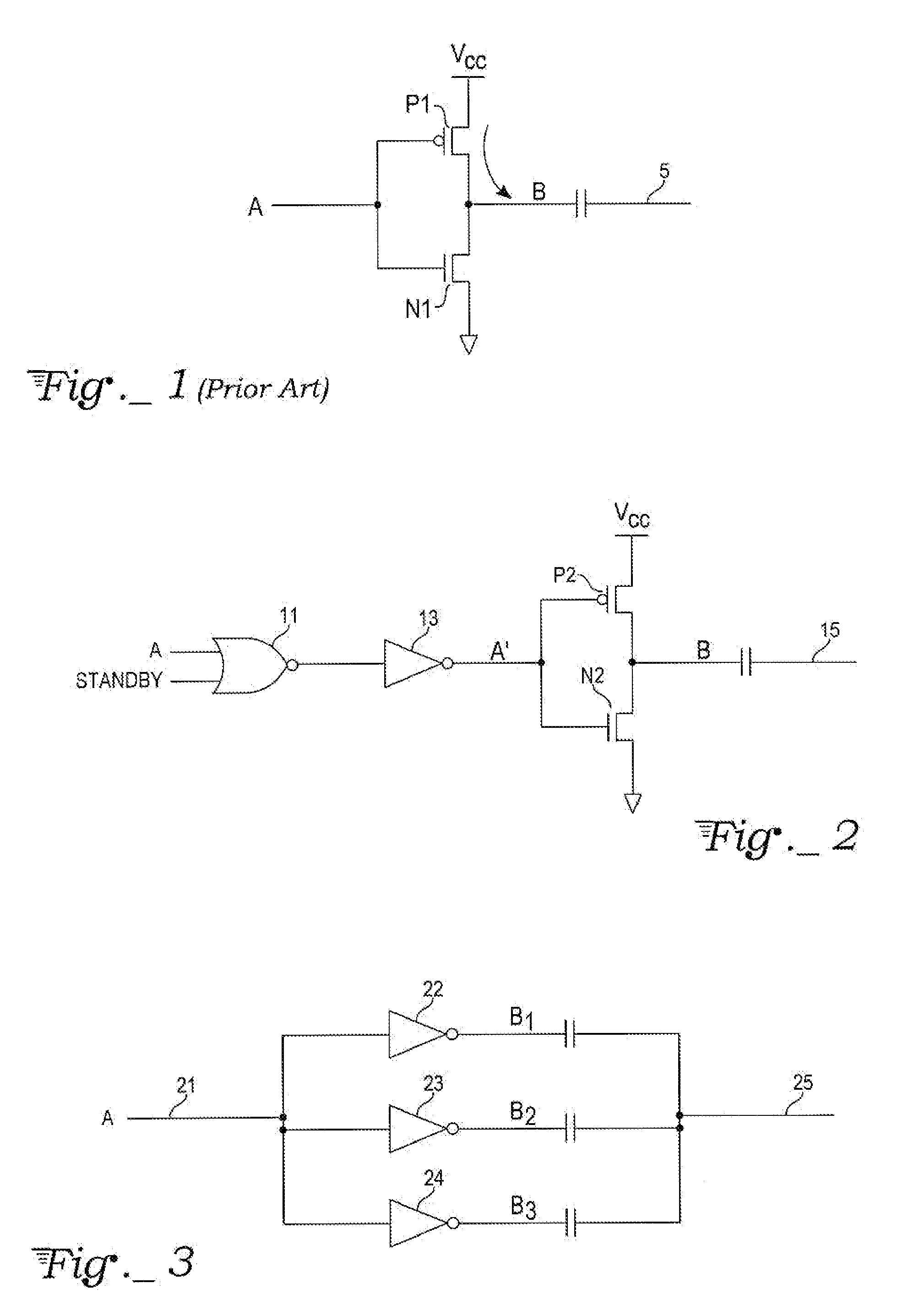
[0006]The present invention eliminates the ESD charge storage problem on high capacitive nodes coupled to an external pin. In particular, the integrated circuit is provided with a logic circuit element, such as a logic gate, responsive to a standby mode signal for generating a control signal that is applied to the gate of a transistor or other active switching element between the external pin and a high capacitive node in order to ensure that in a standby mode, the transistor or active switching element remains off during an ESD test, or during the occurrence of an ESD event, so that the external pin is effectively isolated from the high capacitive node during such ESD test or event. Such a logic circuit element is included at every location in the integrated circuit where a high capacitive node could potentially coupled to an external pin. The added logic circuit element is chosen to be transparent whenever the integrated circuit is not in a standby mode.
[0007]Alternatively or in addition, and wherever possible, the high capacitive node could be broken into many smaller capacitive nodes with duplicate drivers or other active circuit devices connected to the several smaller capacitive nodes in order to eliminate or reduce to a minimum the number of high capacitive nodes needing standby isolation for the ESD test.

Problems solved by technology

Unfortunately, it has been observed that, notwithstanding the presence of ESD protection circuitry manufactured to design specifications, the very act of ESD testing can, under certain circumstances, create damaging hot spots (stored charge) within an integrated circuit.
However, this may not guarantee that the transistor P1 will remain of during an ESD test.
N-channel transistor N1 remains off through the entire test operation and thus does not provide a sink to ground for the charge received and stored at node B. The high capacitive node B discharges only very slowly.
Although the amount of stored charge and its associated voltage is not large enough to immediately damage the devices connected to the high capacitive node—that after all is the main reason for having ESD protection circuitry—if a high voltage at node B were to be sustained for a long enough time, it could stress the connected devices such that junction degradation in those devices is possible.
Current leakage resulting from junction degradation of any devices can cause circuit malfunction under normal operation.

Method used


Image

  • Capacitive node isolation for electrostatic discharge circuit
  • Capacitive node isolation for electrostatic discharge circuit

Examples


Embodiment Construction

[0011]With reference to FIG. 2, a high capacitive node B can be coupled, for example, to a power supply pin VCC via an active switching element of an integrated circuit, e.g., in this embodiment, a p-channel transistor P2 of a CMOS inverter. Likewise, in this exemplary embodiment, the node B can also be coupled to ground pin of the integrated circuit via another active switching element of the circuit, namely an n-channel transistor N2 of the CMOS inverter. When the inverter's input A′ is at a logic 0 level, the p-channel transistor P2 will be on, coupling the VCC pin to the node B, while the n-channel transistor N2 will be off, isolating the node B from ground. Node B will be pulled up to the VCC voltage level. In contrast, when the inverter's input A′ is at a logic 1 level, the p-channel transistor P2 will be off, so that node B is isolated from the VCC pin, while n-channel transistor N2 will be on, coupling the node B to ground. The inverter shown here is merely exemplary of a ci...


PUM


Abstract

Capacitive node isolation circuitry in an integrated circuit eliminates the creation of hot spots (stored charge) on high capacitive nodes during a test of electrostatic discharge (ESD) protection circuitry of the integrated circuit or during any ESD event occurring while the integrated circuit is in a standby mode. The isolation circuitry includes a standby mode logic circuit responsive to a standby mode signal received at one of its inputs and provides an output signal to a gate of an active switching device located in a path between an external pin of the integrated circuit and the internal high capacitive node. The output signal keeps the active switching device turned off for the duration of the ESD test or ESD event. The standby mode logic circuit transparently passes an input logic signal to the active switching device whenever the integrated circuit is in a normal operating mode.

Description

TECHNICAL FIELD[0001]The present invention relates to integrated circuit testing and in particular relates to improvement of electrostatic discharge capabilities of integrated circuits.BACKGROUND ART[0002]Integrated circuits are typically provided with electrostatic discharge (ESD) protection circuitry between the external pins of the device and the main circuit in order to shunt ESD pulses safely to ground and thereby prevent damage to the integrated circuit. Typical ESD pulses can easily exceed 2000 Volts and deliver peak currents of 1 to 30 Amperes within a rapid rise time of 1 to 10 nanoseconds followed by a slow decay in electrical current over the next 100 nanoseconds or so. As a normal part of quality control following integrated circuit manufacture, the ESD protection circuitry is tested. An ESD test normally involves applying a standard electrical waveform representative of one or more ESD events to the various external pins of the manufactured device and observing whether ...

Claims


Application Information

Patent Timeline
IPC IPC(8): H03K19/094
CPCG01R31/002
Inventor NG, PHILIP S.
Owner ATMEL CORP
Learn More