Methods of fabricating ferroelectric devices

a technology of ferroelectric devices and ferroelectric layers, which is applied in the direction of semiconductor devices, electrical devices, capacitors, etc., can solve the problems of low operating speed of fram devices, low efficiency of ferroelectric layers of pzt, and low fatigue characteristics of ferroelectric layers. , to achieve the effect of improving ferroelectric and electrical characteristics, enhancing polarization or data retention, and reducing leakage current density

Active Publication Date: 2008-01-24
SAMSUNG ELECTRONICS CO LTD
View PDF7 Cites 27 Cited by
  • Summary
  • Abstract
  • Description
  • Claims
  • Application Information

AI Technical Summary

Benefits of technology

[0019]Accordingly, in some embodiments, an inactive gas may be provided to a ferroelectric layer formed on a conductive structure or on a lower electrode layer to substantially inhibit a reaction between a remaining gas in the ferroelectric layer formation process and an oxygen-containing gas from forming an impurity layer on the ferroelectric layer. Thus, the ferroelectric layer may have improved ferroelectric and electrical characteristics such as enhanced polarization or data retention, reduced leakage current density, etc. Furthermore, a ferroelectric capacitor including the ferroelectric layer may have improved electrical characteristics.

Problems solved by technology

Volatile semiconductor memory devices may lose data stored therein when power is turned off, whereas nonvolatile semiconductor memory devices can maintain data stored therein after power is turned off.
Currently, the operating speed of FRAM devices may be less than that of DRAM devices due to less advanced techniques for manufacturing FRAM devices.
However, the ferroelectric layer of PZT generally may have relatively poor fatigue characteristics and also may include harmful ingredients, such as lead (Pb).
When a ferroelectric layer including PZT is formed on a substrate by a metal organic chemical vapor deposition (MOCVD) process, the ferroelectric layer may have a rough surface such that the FRAM device including the rough ferroelectric layer may have relatively poor electrical and / or ferroelectric characteristics.
Additionally, charges may be irregularly distributed on the rough surface of the ferroelectric layer which may thereby deteriorate the electrical characteristics of the FRAM device.

Method used


Image

  • Methods of fabricating ferroelectric devices
  • Methods of fabricating ferroelectric devices
  • Methods of fabricating ferroelectric devices

Examples


Embodiment Construction

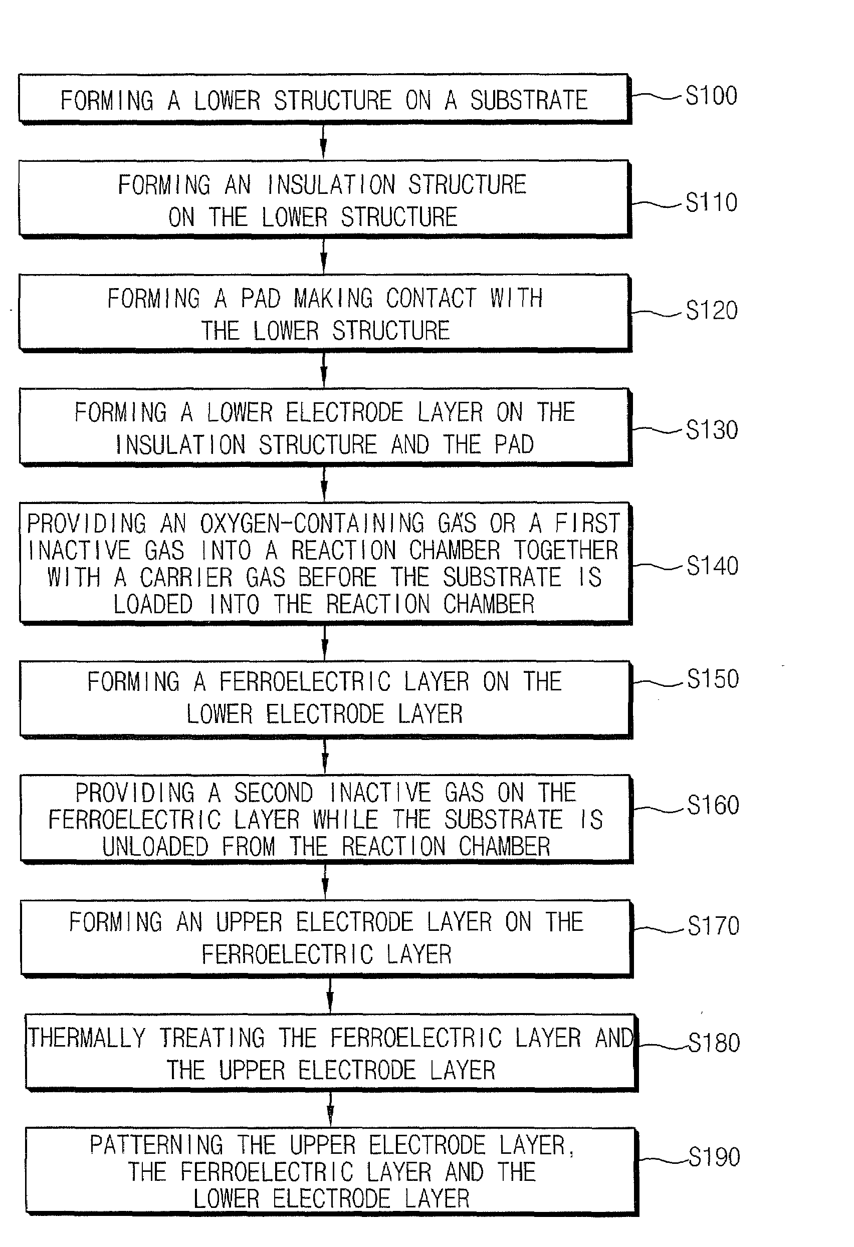
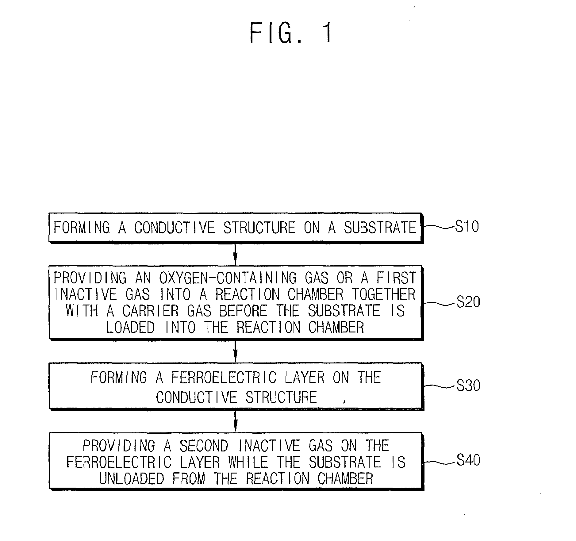
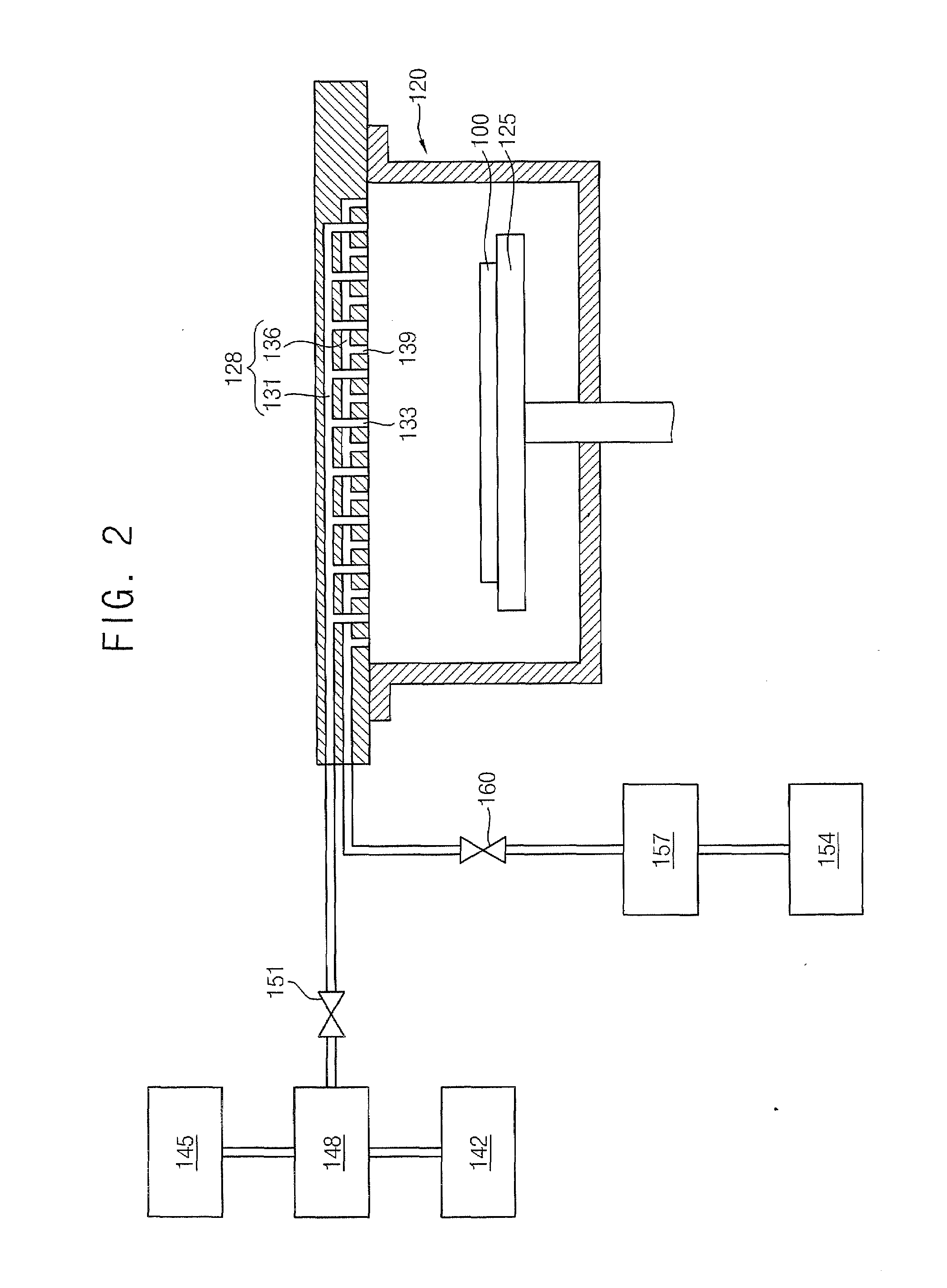
[0027]The present invention is described more fully hereinafter with reference to the accompanying drawings, in which embodiments of the invention are shown. This invention may, however, be embodied in many different forms and should not be construed as limited to the embodiments set forth herein. Rather, these embodiments are provided so that this disclosure will be thorough and complete, and will fully convey the scope of the invention to those skilled in the art. In the drawings, the sizes and relative sizes of layers and regions may be exaggerated for clarity.

[0028]It will be understood that when an element or layer is referred to as being “on,”“connected to” or “coupled to” another element or layer, it can be directly on, connected or coupled to the other element or layer or intervening elements or layers may be present. In contrast, when an element is referred to as being “directly on,”“directly connected to” or “directly coupled to” another element or layer, there are no inte...


PUM

PropertyMeasurementUnit
temperatureaaaaaaaaaa
leakage current densityaaaaaaaaaa

Abstract

A method of fabricating a ferroelectric device includes forming a ferroelectric layer on a substrate in a reaction chamber. An inactive gas is provided into the reaction chamber while unloading the substrate therefrom to thereby substantially inhibit formation of an impurity layer on the ferroelectric layer.

Description

CROSS-REFERENCE TO RELATED APPLICATIONS[0001]This application claims priority under 35 USC § 119 to Korean Patent Application No. 10-2006-0066770 filed on Jul. 18, 2006, the disclosure of which is hereby incorporated by reference herein in its entirety.FIELD OF THE INVENTION[0002]The present invention relates to semiconductor devices, and more particularly, to methods of forming ferroelectric devices and related devices.BACKGROUND OF THE INVENTION[0003]Semiconductor memory devices are generally divided into volatile semiconductor memory devices, such as dynamic random access memory (DRAM) devices and static random access memory (SRAM) devices, and nonvolatile semiconductor memory devices, such as erasable programmable read only memory (EPROM) devices, electrically erasable programmable read only memory (EEPROM) devices and flash memory devices. Volatile semiconductor memory devices may lose data stored therein when power is turned off, whereas nonvolatile semiconductor memory device...

Claims


Application Information

Patent Timeline
Patent Type & Authority Applications(United States)
IPC IPC(8): H01L21/00
CPCH01L28/55H01L21/31691H01L21/02197H01L21/02318H01L21/02271H01L27/04H10B99/00H10B12/00
Inventor IM, DONG HYUNBAE, BYOUNG-JAEKIM, IK-SOOHEO, JANG-EUNLEE, CHOONG-MANYOO, DONG-CHUL
Owner SAMSUNG ELECTRONICS CO LTD
Why Eureka
Try Eureka