
Semiconductor device and driving method therefor

Inactive Publication Date: 2008-01-03
SONY CORP
View PDF3 Cites 6 Cited by
  • Summary
  • Abstract
  • Description
  • Claims
  • Application Information

AI Technical Summary

Benefits of technology

[0021]In the semiconductor device, when the selected storage element (selected cell) is to perform a turning off operation, the second voltage to be applied to the bit line (cathode side) is set higher than the first voltage to be applied to the first region (anode side) of the thyristor. Besides, a positive bias is applied to the gate of the field effect transistor (selected transistor) to turn on the channel so that excessive carriers are swept out rapidly. On the other hand, a voltage lower than the first voltage, for example, where the first voltage is set to a positive voltage, a voltage for placing the field effect transistor into an on state, or a negative voltage, is applied to the word line (gate) for the field effect transistor (selected transistor) of the non-selected storage element (non-selected cell) so that the channel of the field effect transistor is placed into a fully off state. Consequently, a reverse bias voltage from the bit line is prevented from being applied to the thyristor and excessive carries are confined, and therefore, on-information is maintained.
[0022]With the semiconductor device, there is an advantage that, even if the gate of the thyristor is not used, a selected cell and a non-selected cell can be distinguished from each other upon turning off operation, and it is possible to prevent disturbance from a bit line or an anode line and prevent erroneous writing into the non-selected cell. Consequently, the semiconductor device has a high degree of reliability.
[0024]In the driving method for the semiconductor device, when the selected storage element (selected cell) is to perform a turning off operation, the second voltage to be applied to the bit line (cathode side) is set higher than the first voltage to be applied to the first region (anode side) of the thyristor. Besides, a positive bias is applied to the gate of the field effect transistor (selected transistor) to turn on the channel so that excessive carriers are swept out rapidly. On the other hand, a voltage lower than the first voltage, for example, where the first voltage is set to a positive voltage, a voltage for placing the field effect transistor into an on state, or a negative voltage, is applied to the word line (gate) for the field effect transistor (selected transistor) of the non-selected storage element (non-selected cell) so that the channel of the field effect transistor is placed into a fully off state. Consequently, a reverse bias voltage from the bit line is prevented from being applied to the thyristor and excessive carries are confined, and therefore, on-information is maintained.
[0025]With the driving method for the semiconductor device, there is an advantage that, even if the gate of the thyristor is not used, a selected cell and a non-selected cell can be distinguished from each other upon turning off operation, and it is possible to prevent disturbance from a bit line or an anode line and prevent erroneous writing into the non-selected cell. Consequently, the semiconductor device has a high degree of reliability.

Problems solved by technology

As described above, semiconductor devices of the type described above have a problem that, where a bulk silicon wafer is used to form a cell array, a non-selected cell suffers from disturbance from a bit line (or anode line) upon turning from an on state to an off state.

Method used


Image

  • Semiconductor device and driving method therefor
  • Semiconductor device and driving method therefor
  • Semiconductor device and driving method therefor

Examples


first embodiment

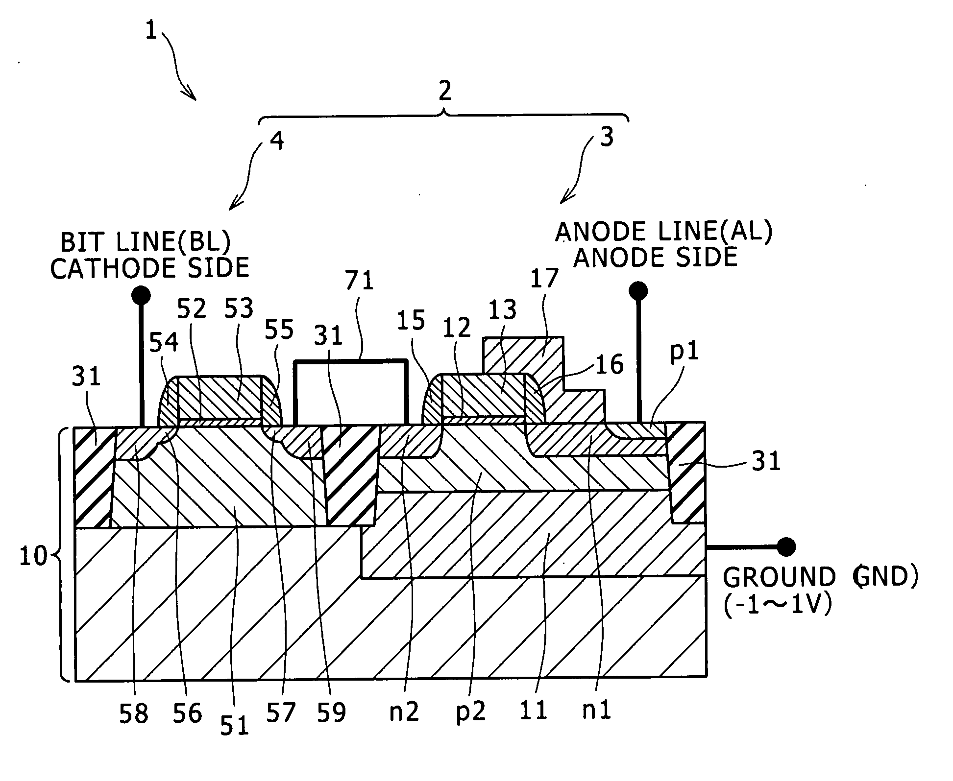
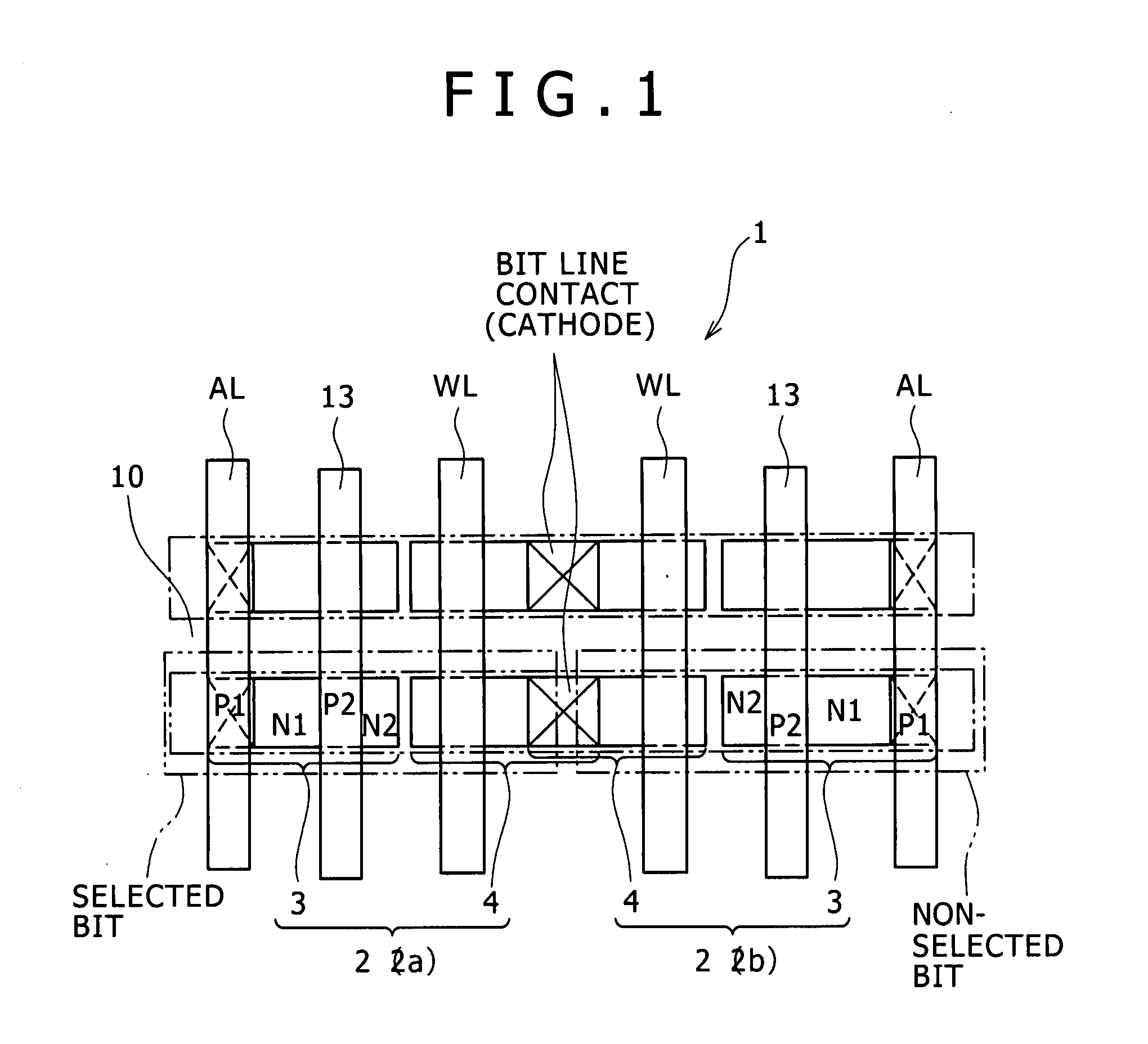
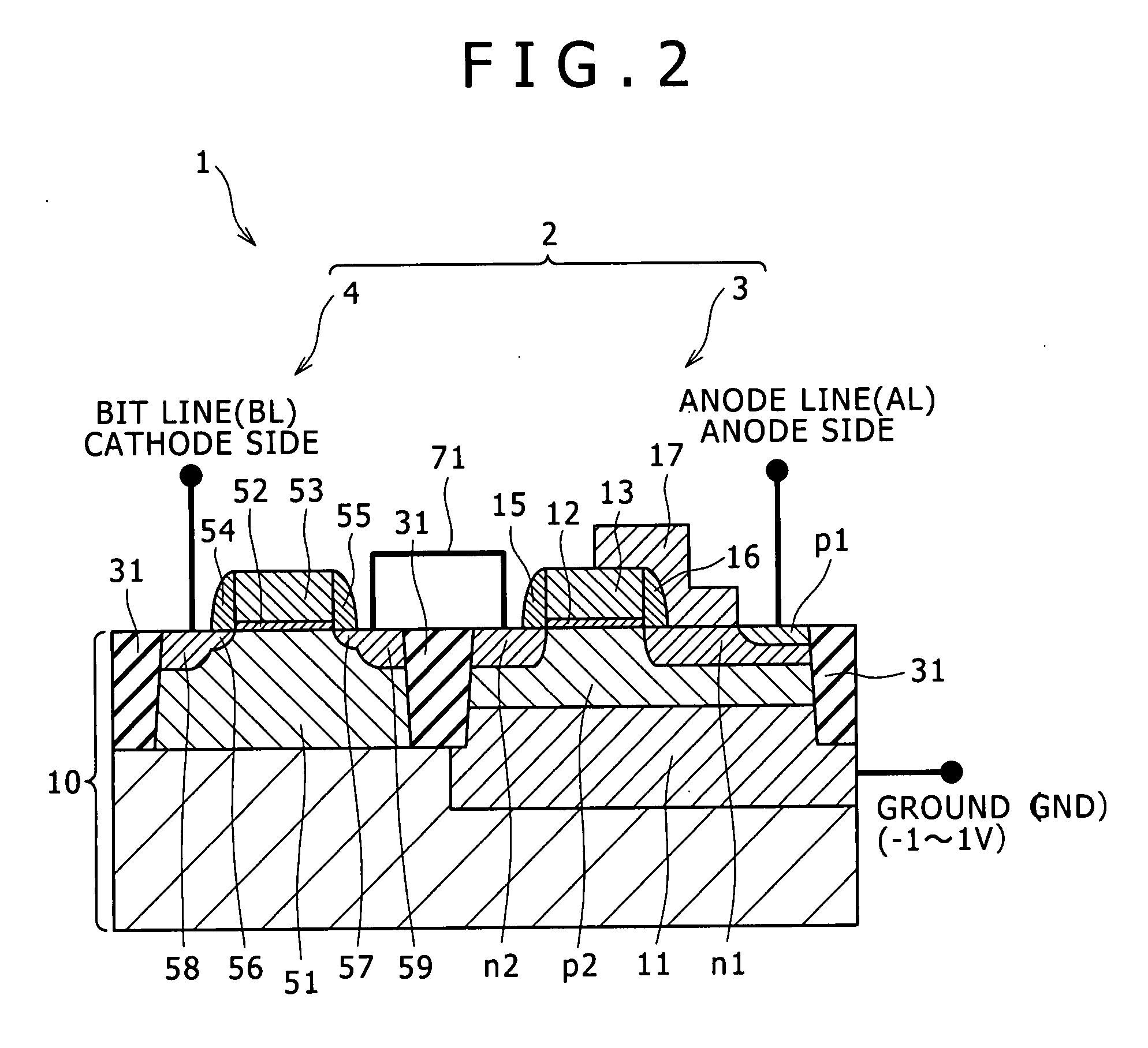
[0051]Now, the semiconductor device 1 of the first embodiment configured such that a gate electrode 13 of a thyristor and a word line WL (gate electrode 53) of a field effect transistor extend perpendicularly to a bit line BL on the layout is described with reference to FIGS. 1, 2 and 3.

[0052]Referring to FIG. 1, such storage elements 2 as described hereinabove with reference to FIG. 2 are arrayed, for example, in a matrix on the bulk semiconductor substrate 10. It is to be noted that the following description is given under the assumption that one (2a) of two storage elements 2 on the same bit line BL corresponds to a selected bit and the other storage element 2 (2b) corresponds to a non-selected bit.

[0053]Referring to FIGS. 1 to 3, in order to turn off (WRITE 0) the selected bit of the semiconductor device 1, a first voltage is applied to the first p-type region p1 side of the thyristor 3 of the selected storage element 2 (selected bit) from between the storage elements 2 while a ...

second embodiment

[0057]Now, another semiconductor device 1 (1b) as the present invention which is configured such that a gate electrode 13 of a thyristor and a word line WL (gate electrode 53) of a field effect transistor extend perpendicularly to an anode line (not shown) on the layout is described with reference to FIGS. 2, 4 and 5.

[0058]Referring to FIG. 4, such storage elements2 as described hereinabove with reference to FIG. 2 are arrayed, for example, in a matrix on the bulk semiconductor substrate 10. The following description is given under the assumption that one of two storage elements 2 on the same bit line BL corresponds to a selected bit and the other storage element 2 corresponds to a non-selected bit.

[0059]Referring to FIGS. 2, 4 and 5, in order to perform a turning off operation (WRITE 0) of the selected bit of the semiconductor device 5, a first voltage is applied to the first p-type region p1 side of the thyristor 3 of the selected storage element 2 (selected bit) from between the ...


PUM


Abstract

A semiconductor device includes a bulk semiconductor substrate, a plurality of storage elements, a bit line, a first voltage being applied to the first region side of the thyristor, and a voltage lower than the first voltage being applied to a word line. The plurality of storage elements formed on the bulk semiconductor substrate and each including a thyristor formed on the bulk semiconductor substrate and including a first region of a first conductor type, a second region of a second conduction type opposite to the first conduction type, a third region of the first conduction type and a fourth region of the second conduction type jointed together in order, a gate electrode formed on the third region, and a field effect transistor formed on the semiconductor substrate on which the thyristor is formed and connected to the fourth region of the thyristor.

Description

CROSS REFERENCES TO RELATED APPLICATIONS[0001]The present invention contains subject matter related to Japanese Patent Application JP 2006-180687 filed with the Japan Patent Office on Jun. 30, 2006, the entire contents of which being incorporated herein by reference.BACKGROUND OF THE INVENTION[0002]1. Field of the Invention[0003]This invention relates to a semiconductor device which switches at a high speed from an on state to an off state and a driving method for the semiconductor device.[0004]2. Description of the Related Art[0005]A memory has been proposed wherein a thyristor is used such that the turn-on and turn-off characteristics of the thyristor are controlled through a gate electrode implemented thereon and the thyristor is connected in series to an access transistor. The memory of the type described is suitable for an SRAM (Static Random Access Memory) and is hereinafter referred to as T-RAM. In a memory operation of the T-RAM, the off region of the thyristor is represente...

Claims


Application Information

Patent Timeline
IPC IPC(8): H01L27/11G11C11/39
CPCG11C11/417H01L21/84H01L27/1203H01L27/11H01L27/1027H10B10/00
Inventor SUGIZAKI, TARO
Owner SONY CORP
Learn More