Semiconductor optical device and manufacturing method thereof
a technology of semiconductors and optical devices, applied in semiconductor devices, semiconductor lasers, lasers, etc., can solve the problems of sharp deterioration of laser characteristics, suppress the diffusion of zn, and reduce the deterioration of crystallinity. , the effect of steep doping profil
- Summary
- Abstract
- Description
- Claims
- Application Information
AI Technical Summary
Benefits of technology
Problems solved by technology
Method used
Image
Examples
embodiment 1
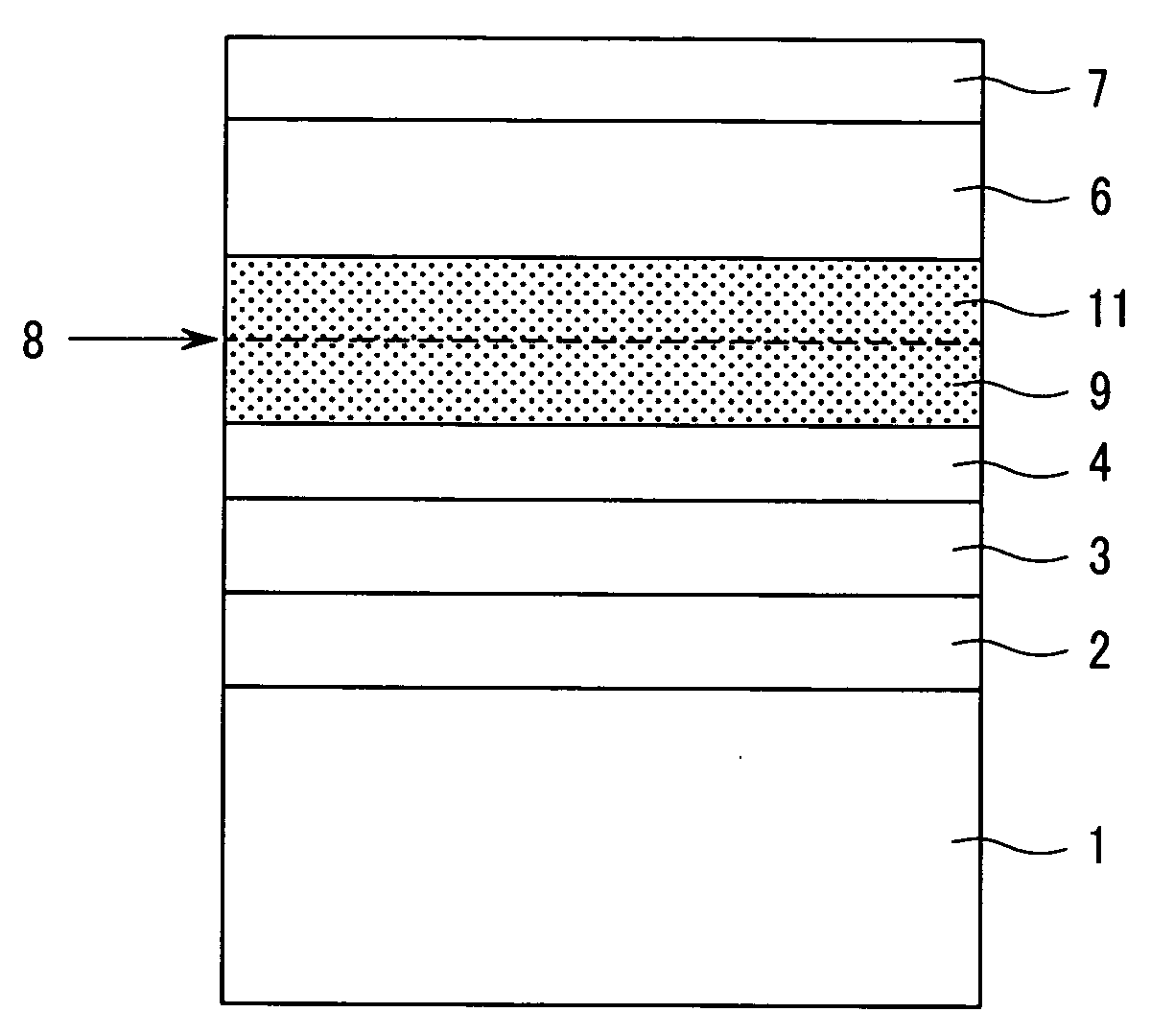
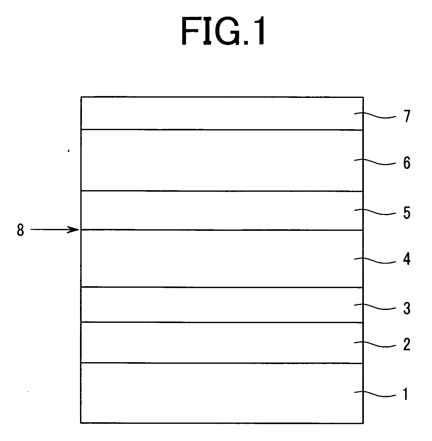
[0027]FIG. 7 shows the cross-sectional structure of the present invention. The following layers are successively grown on an n-InP. substrate 1 by metalorganic vapor phase epitaxy: an n-InP cladding layer 2, an n-InGaAlAs lower-side guiding layer 3, an undoped InGaAlAs multiple quantum well active layer 4, a Zn-doped InGaAlAs upper-side guiding layer 9, a Zn-doped InGaAlAs composition gradient layer (an InGaAlAs layer to an InAlAs layer) 10, a C-doped InAlAs cladding layer (C: 1 to 5×1018 cm−3) 11, a Zn-doped InP cladding layer (Zn: 1×1018 cm−3) 6, and a Zn-doped InGaAs contact layer 7 (Zn: 2×1018 cm−3). The layers up to the Zn-doped InGaAlAs upper-side guiding layer 9 are continuously grown at a growth temperature of 690° C. Then, since it is necessary to lower the growth temperature to 570° C. prior to the growth of the C-doped InAlAs cladding layer 11, the growth interruption 8 is provided. After the growth temperature is stabilized, the C-doped InAlAs cladding layer 11 is grown....
embodiment 2
[0029]FIG. 8 shows an example in which the present invention is applied to a case where the semiconductor optical device includes an upper-side grating layer. When an InGaAsP layer is doped with C, C becomes a p-type dopant in the vicinity of an InGaAs layer and becomes an n-type layer with a low doping concentration (approximately 1×1016 cm−3) in the vicinity of an InP layer. Further, when the InGaAlAs layer is formed of a grating layer, it is necessary to cope with oxidation of a re-growth interface since the grating layer contains Al. Accordingly, with respect to the device structure, an n-InP cladding layer 2, an n-InGaAlAs lower-side guiding layer 3, an undoped InGaAlAs multiple quantum well active layer 4 and a Zn-doped InGaAlAs upper-side guiding layer 9 are grown on an n-InP substrate 1 in the same manner as the above-mentioned embodiment 1. Thereafter, growth interruption by lowering the temperature, growth of a C-doped InAlAs layer 11, growth interruption by increasing the...
embodiment 3
[0030]FIG. 9 shows a case where the present invention is applied to an integrated light source which is formed by a laser and an electro absorption modulator. In the same manner as the above-mentioned embodiment 1, an n-InP cladding layer 2, an n-InGaAlAs lower-side guiding layer 3, an undoped InGaAlAs multiple quantum well active layer 4, a Zn-doped InGaAlAs upper-side guiding layer 9, a C-doped InAlAs cladding layer 11, and a portion of a Zn-doped InP cladding layer are grown on an n-InP substrate 1, forming a laser part 18. Thereafter, using an oxide as a mask, the structure ranging from the surface layer to the substrate is etched by dry etching or wet etching. An n-InGaAlAs lower-side guiding layer 3, an undoped InGaAlAs multiple quantum well active layer 4, an undoped InGaAlAs layer upper-side guiding layer 14, a Zn-doped InGaAlAs upper-side guiding layer 9, a C-doped InAlAs cladding layer 11, and a portion of an InP cladding layer are formed on the removed portion, forming an...
PUM
 Abstract
Description
Claims
Application Information
 - R&D
- Intellectual Property
- Life Sciences
- Materials
- Tech Scout
- Unparalleled Data Quality
- Higher Quality Content
- 60% Fewer Hallucinations
Browse by: Latest US Patents, China's latest patents, Technical Efficacy Thesaurus, Application Domain, Technology Topic, Popular Technical Reports.
© 2025 PatSnap. All rights reserved.Legal|Privacy policy|Modern Slavery Act Transparency Statement|Sitemap|About US| Contact US: help@patsnap.com


