Method of manufacturing a semiconductor integrated circuit and semiconductor integrated circuit

a manufacturing method and integrated circuit technology, applied in the direction of transistors, semiconductor devices, electrical apparatus, etc., can solve the problems of reducing the area and the soi transistor, and achieve the effects of reducing the generation of impact ions, and reducing the electric potential concentration

Inactive Publication Date: 2007-11-01
ABLIC INC
View PDF1 Cites 4 Cited by
  • Summary
  • Abstract
  • Description
  • Claims
  • Application Information

AI Technical Summary

Benefits of technology

[0016] As a result, in the transistor formed on the semiconductor film, a depletion layer generated by a difference in electric potential between a drain and a body can be extended toward the body side in a portion of the drain region having a high density, whereas the depletion layer can be actively extended toward the drain side in a portion of the drain region having a low density. Therefore, the electric potential concentration can be reduced in the vicinity of the body surface of the proximity of the drain and in the vicinity of the embedded insulating film, thereby reducing the generation of impact ions.
[0017] Further, the SOI transistor has a disadvantage in that a method of pulling holes generated by impact ionization out from a body terminal halves the area reduction effect. However, since the generation of impact ions themselves is reduced without providing a body terminal in the SOI transistor according to the present invention, the SOI transistor according to the present invention is effective to realize the area reduction effect which is an advantage of the SOI device.
[0018] Further, according to the present invention, there is provided a method of manufacturing a semiconductor integrated circuit, in which a CMOS transistor is formed on a first conductivity type semiconductor film provided on a first conductivity type supporting substrate through an embedded insulating film, including the steps of: conducting thermal oxidation so as to reach the embedded insulating film to form a LOCOS for element separation between transistors; forming a gate oxide film of a first conductivity type transistor; forming a first conductivity type impurity region reaching the embedded insulating film on the semiconductor film in a region where the first conductivity type transistor is to be formed; forming a polysilicon film serving as a gate electrode of the first conductivity type transistor so as to form a second conductivity type impurity region; forming a second conductivity type impurity region in an ultra-shallow portion of each of a source region and a drain region; forming a second conductivity type impurity region having a low density under the second conductivity type impurity region in the ultra-shallow portion; forming a second conductivity type impurity region having the same density as the second conductivity type impurity region in the ultra-shallow portion under the second conductivity type impurity region having the low density and above the embedded insulating film; providing a mask on the gate electrode and a part of the source region and the drain region so as to form a second conductivity type impurity region in each of the source region and the drain region; forming an interlayer insulating film and forming contact holes in the source region, the drain region, and the gate electrode; and forming a wiring on the interlayer insulating film. In a transistor formed by the above-mentioned method, a width of the portion of the drain region having a low density in a channel length direction is affected by a width of the mask. Therefore, a width in a channel length direction can be more easily controlled as compared with the case where a sidewall is provided around the gate electrode and a portion having a low density is formed in the drain region. As a result, the extension of the depletion layer in the proximity of the drain can be adjusted so as to be uniform. Accordingly, the impact ionization can be reduced in the vicinity of the body surface in the proximity of the drain or in the vicinity of the embedded insulating film.
[0019] Furthermore, according to the present invention, there is provided a method of manufacturing a semiconductor integrated circuit, in which a CMOS transistor is formed on a first conductivity type semiconductor film provided on a first conductivity type supporting substrate through an embedded insulating film, including the steps of: conducting thermal oxidation so as to reach the embedded insulating film to form a LOCOS for element separation between transistors; forming a gate oxide film of a first conductivity type transistor; forming a first conductivity type impurity region reaching the embedded insulating film on the semiconductor film in a region where the first conductivity type transistor is to be formed; forming a first conductivity type impurity region having a higher density than that of the first conductivity type impurity region in a portion of the semiconductor film serving as the proximal region to a drain in the first conductivity type impurity region; forming a polysilicon film serving as a gate electrode of the first conductivity type transistor and forming a second conductivity type impurity region; forming a second conductivity type impurity region in each of the source region and the drain region; forming an interlayer insulating film and forming contact holes in the source region, the drain region, and the gate electrode; and forming a wiring on the interlayer insulating film. In a transistor formed by the above-mentioned method, the depletion layer is extended toward the body side in the portion having a low density of the first conductivity type impurity region in the proximity of the drain while being extended toward the drain side in the portion having a high density so as to allow the uniformization of the extension of the depletion layer in the proximity of the drain. As a result, the generation of impact ions can be reduced. BRIEF DESCRIPTION OF THE DRAWINGS

Problems solved by technology

Further, the SOI transistor has a disadvantage in that a method of pulling holes generated by impact ionization out from a body terminal halves the area reduction effect.

Method used


Image

  • Method of manufacturing a semiconductor integrated circuit and semiconductor integrated circuit
  • Method of manufacturing a semiconductor integrated circuit and semiconductor integrated circuit
  • Method of manufacturing a semiconductor integrated circuit and semiconductor integrated circuit

Examples


first embodiment

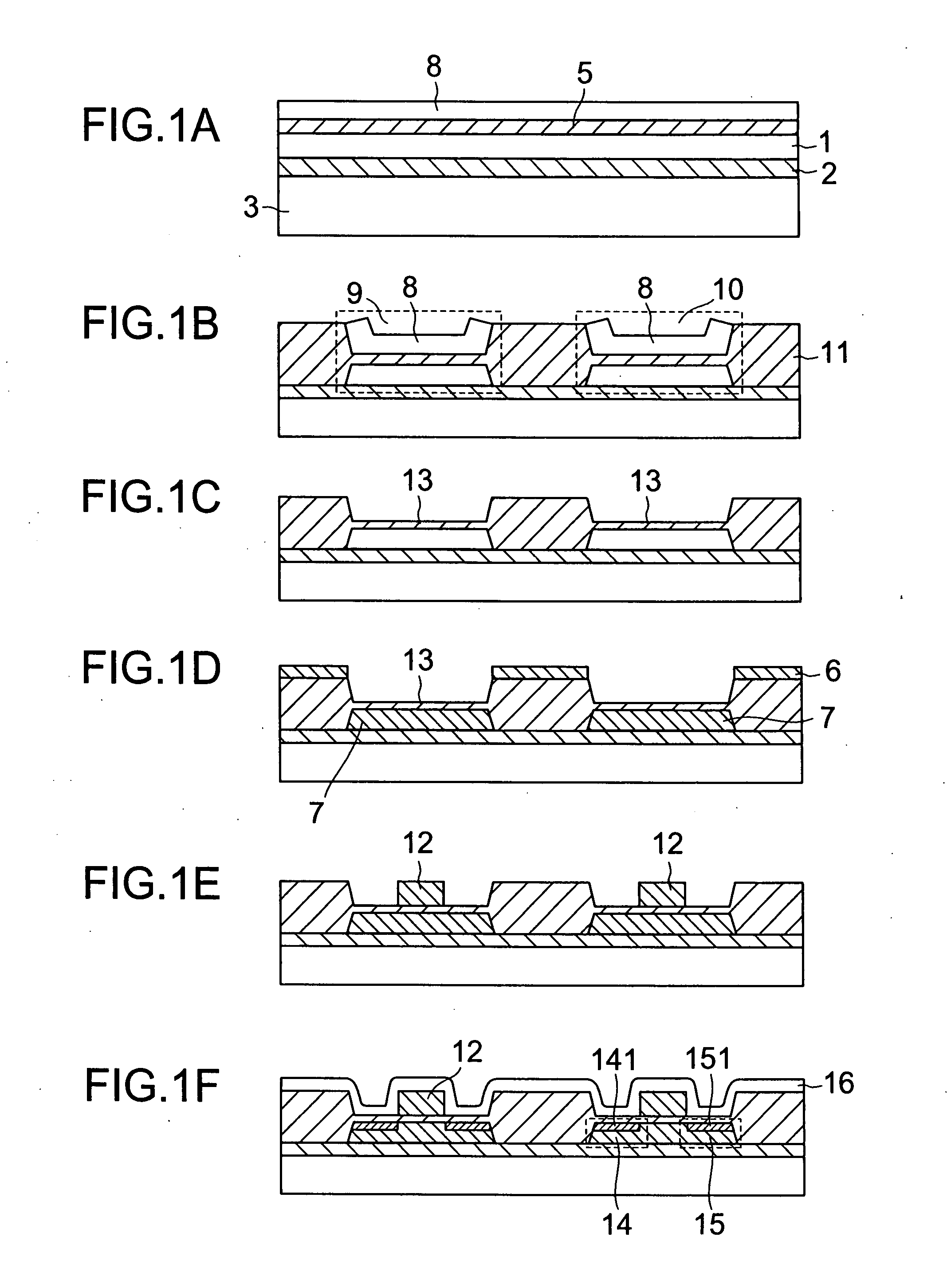
[0034] Hereinafter, the present invention will be described based on FIGS. 1A to 1F and FIGS. 2A to 2F.

[0035] In a method of manufacturing a semiconductor integrated circuit described in the first embodiment of the present invention, a method of manufacturing an N-type transistor and a P-type transistor in a P-type semiconductor film formed on a P-type supporting substrate through an embedded insulating film will be described. The same principle can be applied to a method of forming a transistor in an N-type semiconductor film formed on an N-type supporting substrate through an embedded insulating film. More specifically, two cases are conceived: the case where a first conductivity type is P-type and a second conductivity type is N-type; and the case where a first conductivity type is N-type and a second conductive type is P-type.

[0036] Although only an embodiment for an N-type SOI transistor where the first conductivity type is N-type is described, a P-type SOI transistor formed o...

second embodiment

[0050] Next, the present invention will be described based on FIGS. 7A to 7F and FIGS. 8A to 8F.

[0051] Hereinafter, a method of manufacturing a semiconductor integrated circuit according to the present invention will be described.

[0052] As shown in FIG. 7A, an SOI wafer having the semiconductor film 1 provided on the supporting substrate 3 through the embedded insulating film 2 is thermally oxidized so as to form the thermal oxide film 5 having a thickness of several hundreds of nm. The nitride film 8 is formed thereon to a thickness of about 1600 nm.

[0053] Next, the LOCOS 11 is formed. First, alignment and exposure to light are performed for patterning of the LOCOS 11. Next, the nitride film 8 is etched to form the opening in the LOCOS formation region. The SOI wafer in this state is placed in a thermal oxidation oven so as to form the LOCOS 11. The LOCOS 11 is formed to have such a thickness that the LOCOS 11 reaches the embedded insulating film 2 overlying the supporting substr...

third embodiment

[0065] Next, the present invention will be described based on FIGS. 11A to 11F and FIGS. 12A to 12C. Hereinafter, a method of manufacturing a semiconductor integrated circuit according to the present invention will be described.

[0066] As shown in FIG. 11B, the LOCOS 11 is formed in an SOI wafer having the semiconductor film 1 provided on the supporting substrate 3 through the embedded insulating film 2. First, the thermal oxide film 5 is formed to a thickness of several hundreds of angstrom. The nitride film 8 is formed thereon to a thickness of about 1600 angstrom. Next, alignment and exposure to light are performed for patterning of the LOCOS 11. Then, the nitride film 8 is etched to form the opening in the LOCOS formation region. FIG. 11A shows a state where a mask of the thermal oxide film 5 and the nitride film 8 is formed on the P-type transistor region 9 and the N-type transistor region 10. The SOI wafer in this state is placed in a thermal oxidation oven so as to form the LO...


PUM


Abstract

Conventionally, when an electric potential of a supporting substrate is fixed, there arises a problem in that impact ions are generated even in the vicinity of embedded insulating film in the proximity of a drain due to generation of a parasitic transistor using the supporting substrate as a gate so as to be likely to cause a parasitic bipolar operation. A method of the present invention includes the steps of: forming and patterning a LOCOS reaching an embedded insulating film, a gate oxide film, a well and a polysilicon film serving as a gate electrode; forming a second conductivity type high-density impurity region in an ultra-shallow portion of each of a source region and a drain region, a second conductivity type impurity region having a low density under the second conductivity type high-density impurity region of the ultra-shallow portion, and a second conductivity type impurity region having a high density under the second conductivity type impurity region having a low density and above the embedded insulating film; forming a sidewall around the gate electrode; forming a second conductivity type impurity region in each of the source region and the drain region; forming an interlayer insulating film and forming contact holes in the source region, the drain region and the gate electrode; and forming a wiring on the interlayer insulating film.

Description

BACKGROUND OF THE INVENTION [0001] 1. Field of the invention [0002] The present invention relates to a method of manufacturing a transistor having a structure allowing the reduction of impact ionization in a transistor formed on an SOI wafer. In particular, the present invention relates to a method of manufacturing an SOI transistor having an electric potential of a supporting substrate fixed to a GND level or a low voltage level. [0003] 2. Description of the Related Art [0004]FIGS. 4A to 4D show a method of manufacturing a conventional SOI transistor, and FIGS. 5A and 5B are a top view and a cross-sectional view showing a structure of the conventional SOI transistor. Herein, the transistor is formed by using a wafer in which a P-type semiconductor film is formed on a P-type supporting substrate through an embedded insulating film. [0005] The conventional SOI transistor is formed in a semiconductor film 1 surrounded by a LOCOS 11 reaching an embedded insulating film as shown in FIG....

Claims


Application Information

Patent Timeline
Patent Type & Authority Applications(United States)
IPC IPC(8): H01L21/8238H01L27/08H01L21/336H01L21/762H01L21/84H01L27/092H01L27/12H01L29/786
CPCH01L21/76264H01L21/76281H01L21/823814H01L21/84H01L29/78624H01L29/66772H01L29/78612H01L29/78621H01L27/1203
Inventor WAKE, MIWAYOSHIDA, YOSHIFUMI
Owner ABLIC INC
Why Eureka
Try Eureka