
Dual damascene process

a damascene and process technology, applied in the direction of semiconductor/solid-state device manufacturing, basic electric elements, electric devices, etc., can solve the problems that the most dual damascene process still has a number of technical problems, and achieve the effect of greater control

Inactive Publication Date: 2007-10-25
UNITED MICROELECTRONICS CORP
View PDF7 Cites 9 Cited by
  • Summary
  • Abstract
  • Description
  • Claims
  • Application Information

AI Technical Summary

Benefits of technology

The present invention provides a dual damascene process that allows for better control over the depth of a trench and opening when a trench and an opening are formed together. The process includes sequentially forming layers over a substrate, using a patterned hard mask layer as a mask to remove a portion of the dielectric layer and expose a portion of the etching stop layer. A filling material layer is then deposited over the substrate, with the surface of the filling material layer being lower than the top of the opening. The process also includes using a patterned photoresist layer to form the first opening and using an anti-reflection layer to improve the process. The invention also provides a method for forming a trench and opening in a dielectric layer using a dual damascene process.

Problems solved by technology

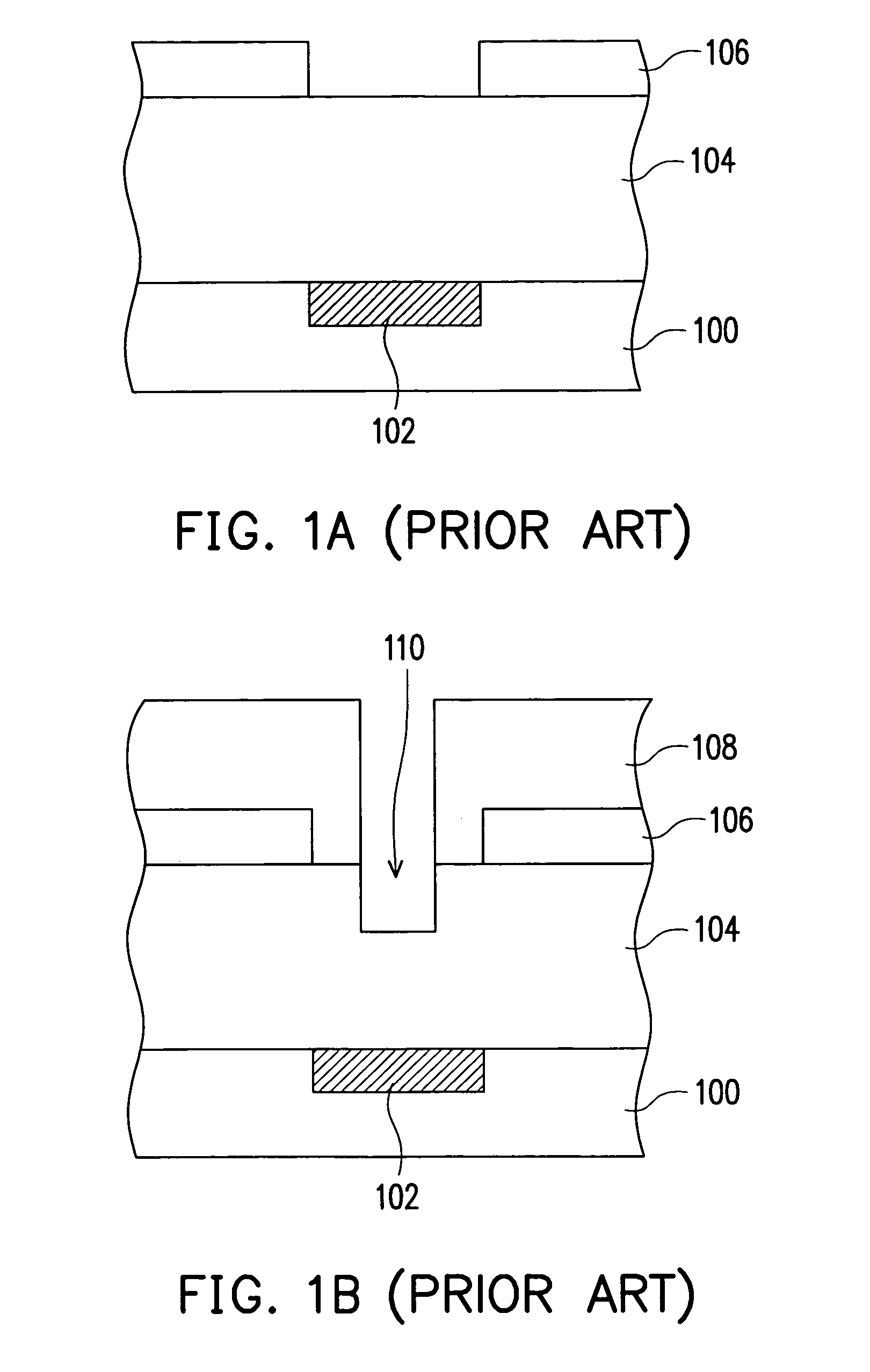
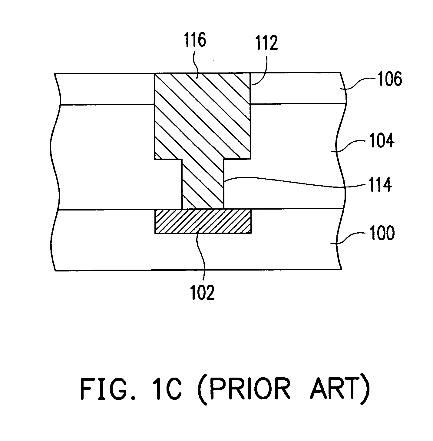
However, most dual damascene processes still has a number of technical problems. FIGS. 1A through 1C are schematic cross-sectional views showing the steps in a conventional dual damascene process.

Method used


Image

  • Dual damascene process
  • Dual damascene process
  • Dual damascene process

Examples


Embodiment Construction

[0038] Reference will now be made in detail to the present preferred embodiments of the invention, examples of which are illustrated in the accompanying drawings. Wherever possible, the same reference numbers are used in the drawings and the description to refer to the same or like parts.

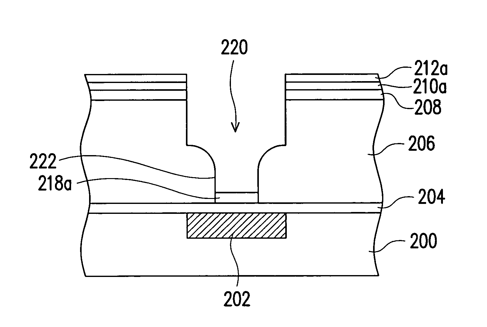
[0039]FIGS. 2A through 2E are schematic cross-sectional views showing the steps in a dual damascene process according to one embodiment of the present invention. First, as shown in FIG. 2A, a substrate 200 having a conductive area 202 thereon is provided. The conductive area 202 is a conductive wire or an electrode formed in a conventional interconnection process, for example. Then, an etching stop layer 204 is formed over the substrate 200. The etching stop layer 204 is a silicon carbonitride layer formed by performing a chemical vapor deposition (CVD) process. Thereafter, a dielectric layer 206 is formed over the etching stop layer 204. The dielectric layer 206 is formed using a low dielectric co...


PUM

PropertyMeasurementUnit
conductiveaaaaaaaaaa
dielectricaaaaaaaaaa
dielectric constantaaaaaaaaaa

Abstract

A dual damascene process is provided. A substrate having a conductive area is provided. An etching stop layer, a dielectric layer and a patterned hard mask layer are sequentially formed on the substrate. A first opening is formed in the dielectric layer exposed by the patterned hard mask layer. A first material layer having a high etching selectivity with respect to the dielectric layer is deposited to fill the first opening. A portion of the dielectric layer and the filling material layer are removed to form a trench and a second opening. The filling material layer exposed by the second opening is removed to expose part of the etching stop layer. A portion of the etching stop layer is removed to form a third opening. A conductive layer is formed in the trench and the third opening.

Description

BACKGROUND OF THE INVENTION [0001] 1. Field of the Invention [0002] The present invention relates to a semiconductor fabrication process. More particularly, the present invention relates to a dual damascene process. [0003] 2. Description of the Related Art [0004] Dual damascene process is a technique for embedding interconnects within an insulating layer. The deployment of the dual damascene process can avoid overlay error and process bias problem that results from forming metallic wires in a photolithographic process after forming a contact. Furthermore, the dual damascene process can improve the reliability of the devices and increase the productivity of the production processes. Consequently, as the level of device integration continues to increase, the dual damascene process has gradually become one of the principle techniques for forming integrated circuits in the semiconductor industry. [0005] However, most dual damascene processes still has a number of technical problems. FIG...

Claims


Application Information

Patent Timeline
Patent Type & Authority Applications(United States)
IPC IPC(8): H01L21/4763
CPCH01L21/76811
Inventor HUANG, CHUN-JENWENG, CHENG-MINGWANG, MENG-JUN
Owner UNITED MICROELECTRONICS CORP
Learn More