Method for manufacturing a semiconductor device having a nitrogen-containing gate insulating film
- Summary
- Abstract
- Description
- Claims
- Application Information
AI Technical Summary
Benefits of technology
Problems solved by technology
Method used
Image


Examples
Embodiment Construction
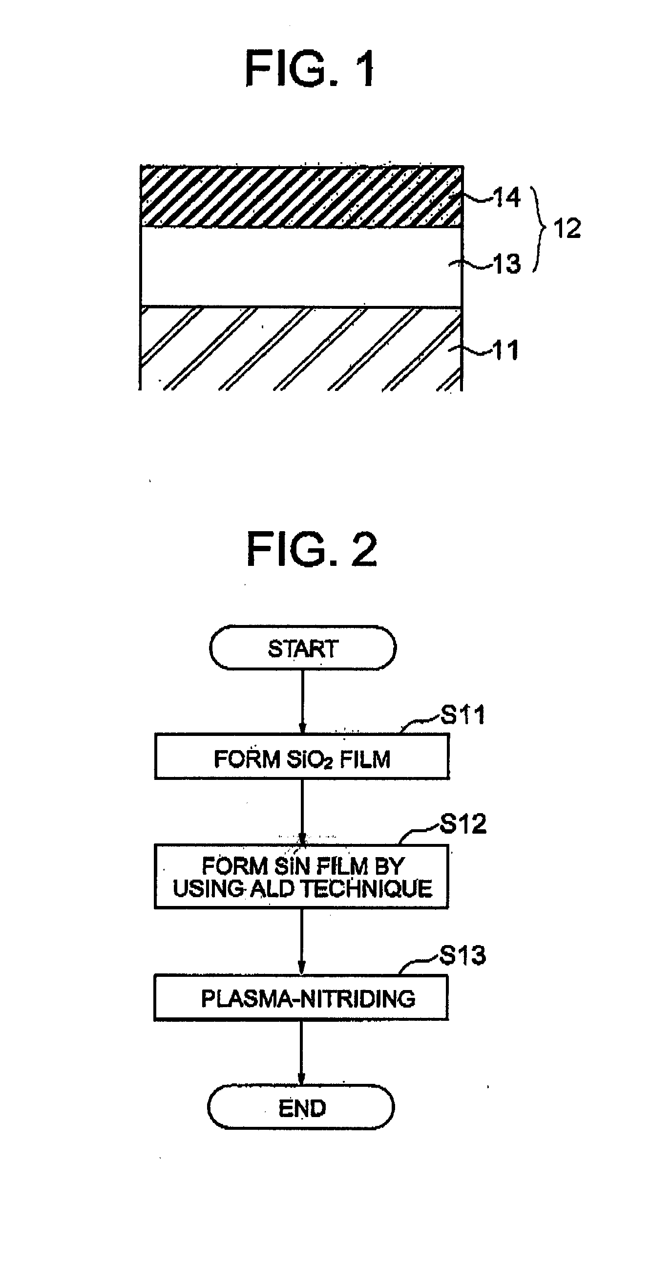
[0021]An embodiment of the present invention will be described in further detail with reference to the accompanying drawings. FIG. 1 is a sectional view showing the layer structure of a gate insulating film formed by a method for manufacturing a semiconductor device according to the embodiment of the invention. The gate insulating film 12 includes a SiO2 film 13 and a SiN film 14 consecutively layered on a silicon substrate 11. Agate electrode made of doped polysilicon (not shown) is formed on the gate insulating film 12. Instead of the doped polysilicon, titanium nitride (TiN) or nickel silicide NiSi) may be used for the gate electrode.
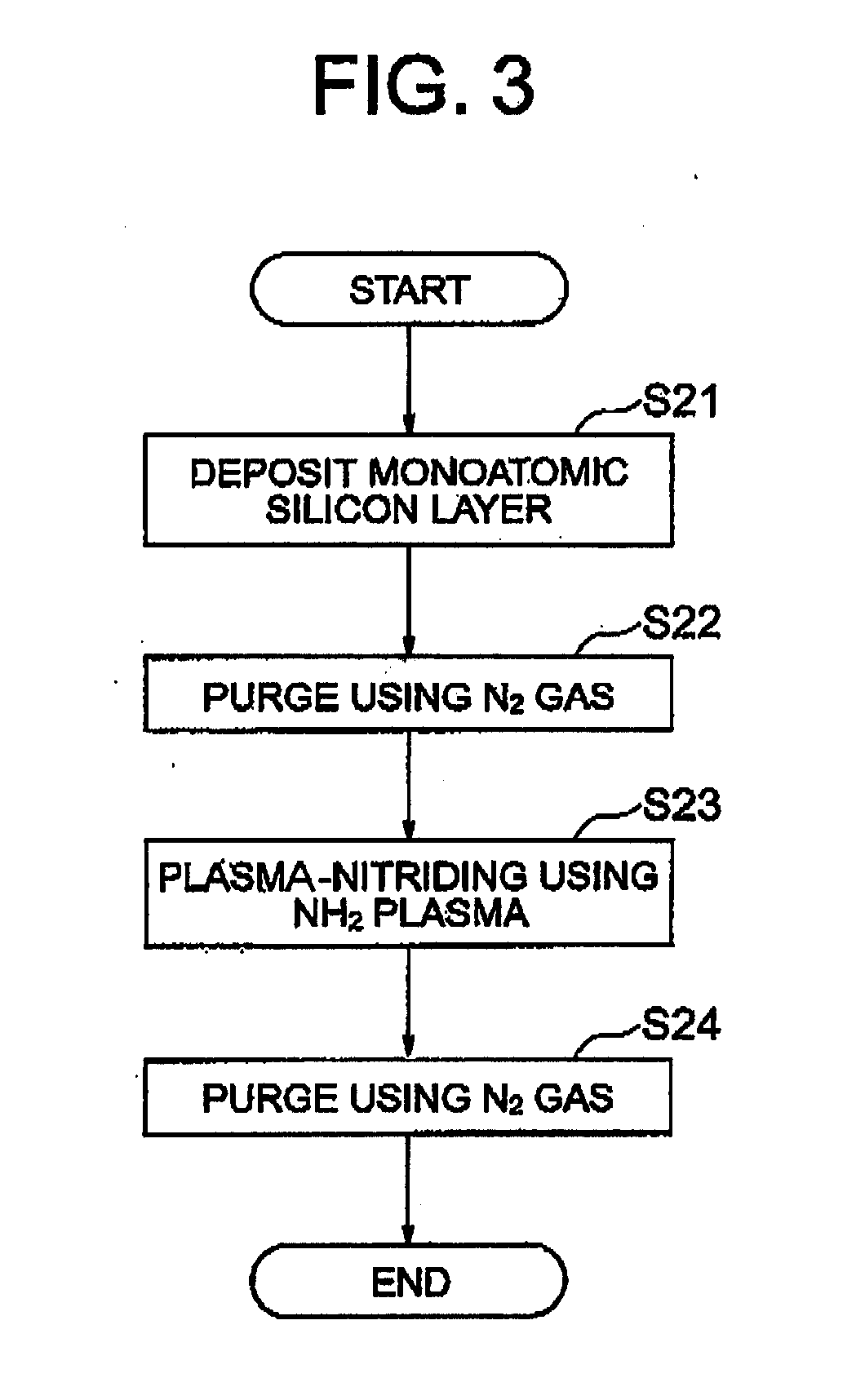
[0022]FIG. 2 is a flowchart showing a process of forming the gate insulating film 12 shown in FIG. 1. After an isolation structure (not shown) is formed on the surface portion of the silicon substrate 11, a thermal oxidation process is used to form the SiO2 film 13 on the silicon substrate 11 (Step S11). The resultant wafer (silicon substrate) is the...
PUM
 Abstract
Description
Claims
Application Information
 - R&D
- Intellectual Property
- Life Sciences
- Materials
- Tech Scout
- Unparalleled Data Quality
- Higher Quality Content
- 60% Fewer Hallucinations
Browse by: Latest US Patents, China's latest patents, Technical Efficacy Thesaurus, Application Domain, Technology Topic, Popular Technical Reports.
© 2025 PatSnap. All rights reserved.Legal|Privacy policy|Modern Slavery Act Transparency Statement|Sitemap|About US| Contact US: help@patsnap.com