
Structure and method for controlling the behavior of dislocations in strained semiconductor layers

a technology of dislocation and semiconductor layer, applied in the direction of semiconductor devices, basic electric elements, electrical apparatus, etc., can solve the problems of device failure associated with crystal defects, little s/d region left to use, and the extent and integrability of such approaches becomes quite difficult, so as to reduce the probability of shorting the s/d region of fets and reduce the effect of diffusion

Inactive Publication Date: 2007-09-20
GLOBALFOUNDRIES INC
View PDF5 Cites 3 Cited by
  • Summary
  • Abstract
  • Description
  • Claims
  • Application Information

AI Technical Summary

Benefits of technology

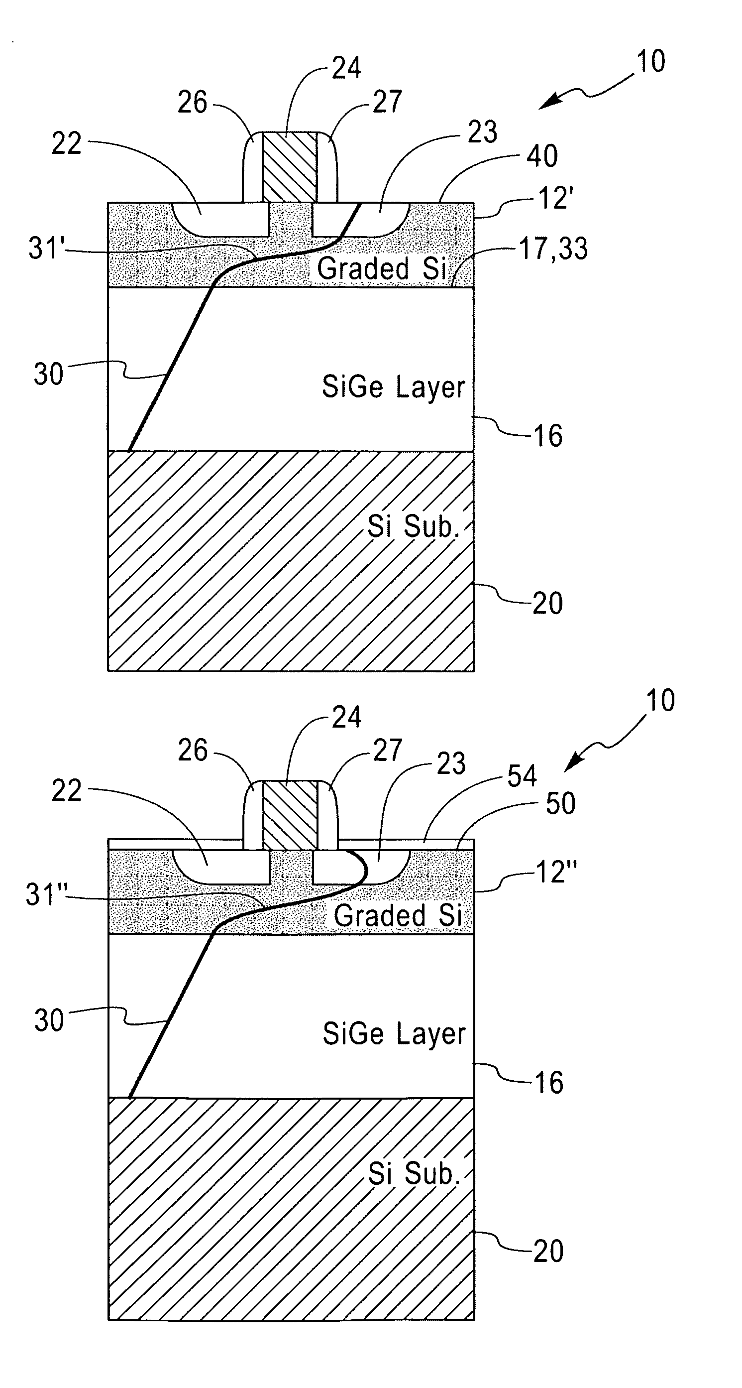
[0008] The invention described herein pertains to a particular strain-graded topmost layer, grown on the SiGe buffer layer, which provides 1) a Si surface for the transistor channel region and 2) a strain vs. depth profile that makes the region where interfacial dislocation segments are created far enough below the surface to be beneath the S / D regions thereby reducing the probability of shorting the S / D regions of FETs. An additional benefit of creating a strain-graded cap layer is that the Ge concentration can be made to be a smooth function of depth which limits Ge diffusion into the Si channel region and also reduces dopant diffusion.
[0009] Another embodiment of the present invention contemplates the deliberate micro-roughening of the upper surface of the strained semiconductor layer. This embodiment provides a method of pinning the motion of the dislocations by creating a barrier to dislocation glide. The deliberate micro-roughening can be performed everywhere on the exposed surface or in pre-specified non-critical regions of the surface to act as localized dislocation traps. The advantage of the roughened surface is that it can be used to increase the critical thickness of the strained layer at a given Ge concentration or gradient.

Problems solved by technology

The main problem with local strain techniques is that as the device pitch (spacing between devices) decreases, the extent and integrability of such approaches becomes quite challenging; there is very little S / D region left to use.
The main challenge to global strain Si has been the device failures associated with crystal defects.
Low-defect compositionally-graded SiGe layers have been demonstrated to have 105 dislocations / cm2 as well as low-defect silicon germanium on insulator (SGOI), however, after growing the strained Si layer on the SiGe alloy, the dislocations can glide in the strained Si layer and leave behind a misfit dislocation segment along the Si / SiGe interface.
Such very thin layers are prohibitively thin for current CMOS fabrication.
However, because of the enhanced dopant diffusion of As or P in SiGe, the S / D formation is less controlled after ion implantation and S / D activation annealing.

Method used


Image

  • Structure and method for controlling the behavior of dislocations in strained semiconductor layers
  • Structure and method for controlling the behavior of dislocations in strained semiconductor layers
  • Structure and method for controlling the behavior of dislocations in strained semiconductor layers

Examples


Embodiment Construction

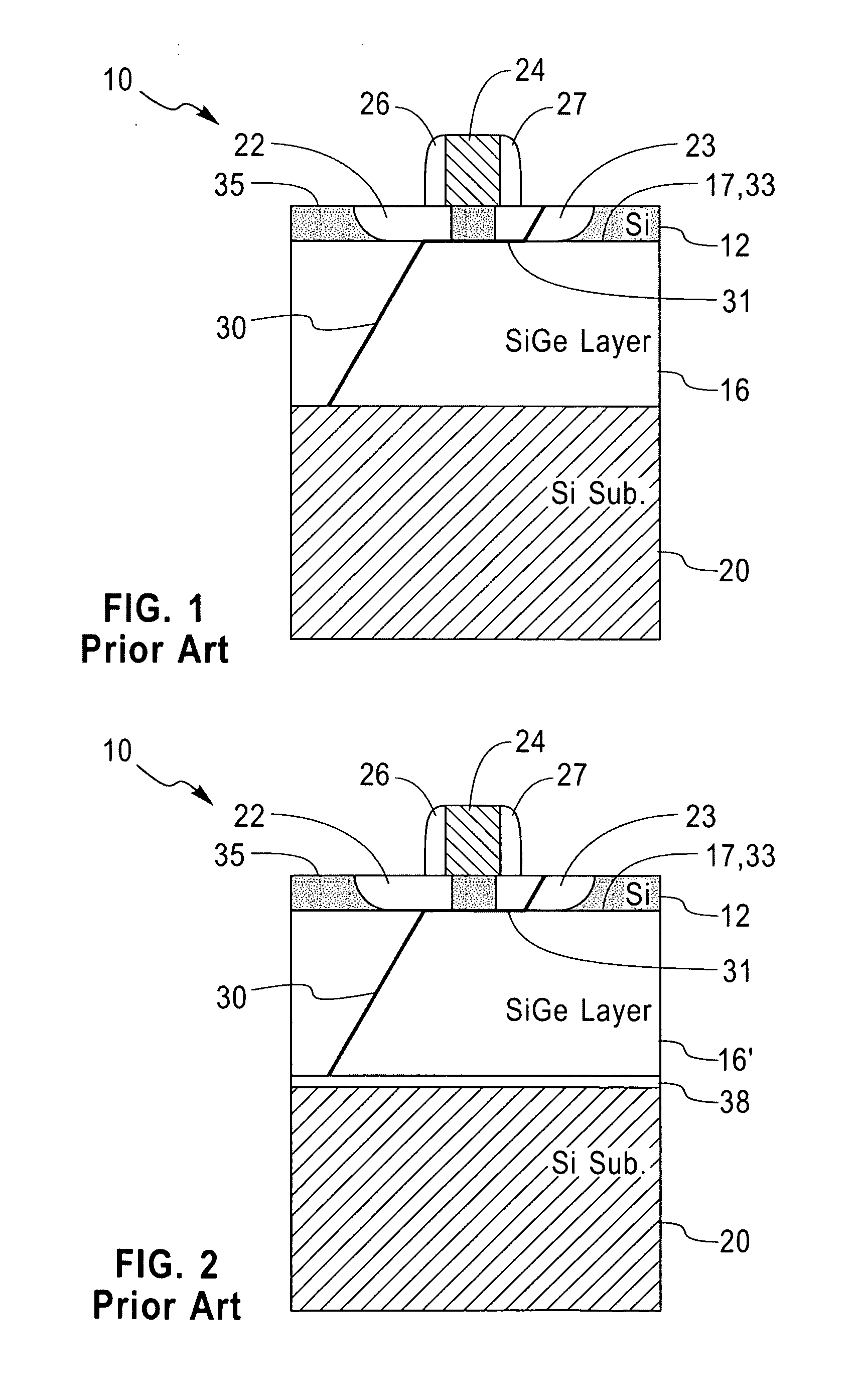
[0017]FIG. 1 shows a cross section view of a MOSFET 10 formed on a strained semiconductor layer 12 which may be Si or Si containing. Strained layer 12 is formed over a SiGe layer 16 which in turned is formed over a substrate 20. Strained layer 12 may be formed by epitaxial deposition over SiGe layer 16. SiGe layer 16 may be epitaxially deposited over substrate 20 which may be single crystalline. The amount of Ge in layer 16 may be increased with layer thickness and then relaxed to form a crystal lattice spacing greater than the future lower surface of layer 12 to cause global bidirectional strain in layer 12. Thus, layer 16 may be graded SiGe up to the upper surface 17 of layer 16. Layer 12 may be of constant Si or SiGe composition.

[0018] Alternatively in place of SiGe graded layer 16, layer 16 may be a Silicon Germanium on Insulator (SGOI) as shown in FIG. 2.

[0019] In FIGS. 1-5, MOSFET 10, has a source 22, drain 23 and gate 24. Sidewall spacers 26 and 27 are also present. Source ...


PUM


Abstract

A structure and method for controlling the behavior of dislocations in strained semiconductor layers is described incorporating a graded alloy region to provide a strain gradient to change the slope or curvature of a dislocation propagating upwards or gliding in the semiconductor layer in the proximity of the source and drain of a MOSFET. The upper surface of the strained semiconductor layer may be roughened and / or contain a dielectric layer or silicide which may be patterned to trap the upper end of dislocations in selected surface areas. The invention solves the problem of dislocation segments passing through both the source and drain of a MOSFET creating leakage currents or shorts therebetween.

Description

FIELD OF THE INVENTION [0001] This invention relates to strained semiconductor layers for forming integrated circuit chips and more particularly to controlling the behavior of dislocations in strained semiconductor layers. BACKGROUND OF THE INVENTION [0002] Forming metal oxide semiconductor field-effect transistors (MOSFETs) on Si layers under tensile strain allows for the continued development of high-performance / low-power CMOS integrated circuits. The enhanced charge carrier mobility in strained Si compared to unstrained Si allows for the increase of on-state transistor current without the need to decrease the physical dimensions of the device; which is becoming increasingly more difficult to do. For strained Si applications, the two main approaches used to create strain in the transistor channel region are 1) growing a thin Si layer on a relaxed SiGe alloy layer (global strain) and 2) straining the channel region using integrated circuit (IC) process-level techniques such as refi...

Claims


Application Information

Patent Timeline
IPC IPC(8): H01L21/8232H01L21/335
CPCH01L21/823807H01L29/7843H01L29/78H01L29/1054
Inventor BEDELL, STEPHEN W.DESOUZA, JOEL P.SADANA, DEVENDRA K.SCHWARZ, KLAUS W.REZNICEK, ALEXANDER
Owner GLOBALFOUNDRIES INC
Learn More