Method for forming dielectric or metallic films

a dielectric or metallic film technology, applied in the direction of coatings, chemical vapor deposition coatings, semiconductor devices, etc., to achieve the effect of excellent conductivity and excellent properties

Inactive Publication Date: 2007-08-16
LAIR LIQUIDE SA POUR LETUDE & LEXPLOITATION DES PROCEDES GEORGES CLAUDE
View PDF20 Cites 21 Cited by
  • Summary
  • Abstract
  • Description
  • Claims
  • Application Information

AI Technical Summary

Benefits of technology

[0014] It is an aim of the invention to provide methods and compositions that satisfy the need to form a thin film with excellent electrical qualities and high conformality, and which avoid using multiple forming steps to obtain uniform coverage and high conformality. Another aim of the invention is to provide a film that minimizes chlorine and carbon contents, both of which can degrade the electrical properties of the film. A further aim of the invention is to provide the ability to control the M / Si ratio in the films over a broad range without changing precursor solutions. Still another aim is to avoid quality and conformality issues that can occur when vaporizing a liquid precursor solution containing multiple components or bubbling a carrier gas through a liquid silicon source.
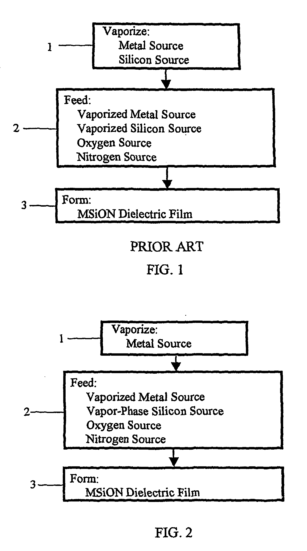
[0016] According to a preferred embodiment, a vapor phase silicon precursor and a liquid phase metal precursor are used for the deposition of films having the desired stoichiometry. The vapor phase silicon precursor has to be sufficiently volatile at temperatures above 15° C. to supply the process as a vapor avoiding the bubbling of a carrier gas through a liquid or heating in a vaporizer. This eliminates the control and quality problems associated with the vaporization of two precursors (a metal containing precursor and a silicon containing precursor) or bubble a carrier gas through a liquid to feed the silicon source. In addition, the vapor phase silicon precursor is not coordinated to a metal allowing independent control over feeding of the metal source and the silicon source. Thus, the M / Si ratio can be easily varied over a wide range without having to mix new precursor solutions and recalibrate the process to the new precursor mixture. Furthermore, the vapor phase silicon precursor is carbon and chlorine free, hence dramatically reducing the undesirable effects of carbon and chlorine in the dielectric film. Finally, according to the invention a dielectric film of the desired final composition is produced in a single step.
[0029] The reaction of the precursors in the deposition chamber leads to the formation of a film on the silicon substrate. The composition of the film can be precisely controlled by precisely controlling the flow rates of each of the precursors independently. The feed rates of the silicon and metal sources are independently controllable, thus the M / Si ratio of the resulting film is controllable over a wide range without changing the composition of the metal source or the silicon source.
[0031] Because the silicon, oxygen and nitrogen sources in this invention are all carbon and chlorine free, the resulting film has excellent properties, i.e. a high dielectric constant for gate dielectrics or excellent conductivity as for metallic films.

Problems solved by technology

In addition, the vapor phase silicon precursor is not coordinated to a metal allowing independent control over feeding of the metal source and the silicon source.

Method used


Image

  • Method for forming dielectric or metallic films
  • Method for forming dielectric or metallic films
  • Method for forming dielectric or metallic films

Examples


example 1

[0071] This example relates to the manufacture of hafnium silicon oxynitride films. The CVD tool used in this example is illustrated in FIG. 6. In FIG. 6, a silicon wafer 1 is mounted in a CVD chamber 11 that is provided with a heater over its circumference and the desired film is formed on the surface of the silicon wafer 1. The CVD chamber 11 is evacuated by a pump 12. The metal precursor, in this case tetrakisdiethylaminohafnium Hf(NEt2)4, is stored in a liquid container 21. Helium gas 22 is used as the carrier gas for the Hf(NEt2)4. The Hf(NEt2)4 in the liquid container 21 is transported by the pressure of the helium 22 through a liquid mass flow controller 23 and into a vaporizer 25. Helium 22 is also transported through a mass flow controller 24 into the vaporizer 25. The Hf(NEt2)4 vaporized by the vaporizer 25 is fed to the CVD chamber 11 along with He. Trisilylamine (TSA) is held in a bottle 31, and this TSA is transported through a mass flow controller 32 to the CVD chamber...

example 2

[0078] This example relates to the manufacture of hafnium silicon oxide film. The CVD tool used in this example is illustrated in FIG. 7. The CVD tool in FIG. 7 has a structure very similar to that of the CVD tool illustrated in FIG. 1, differing from the latter in that a bubbler 43 filled with H20 is provided along the course of the O2 gas 42 line, resulting in the feed into the CVD chamber 11 of H2O along with O2 as the oxidizing agent. Hafnium silicon oxide film was produced under the following conditions using the described CVD tool.

Mode 2-1

[0079] Pressure=0.5 torr, temperature=400° C., Hf(NEt2)4 flow rate=0.5 sccm, He flow rate=160 sccm, TSA flow rate=4 sccm, O2 flow rate=40 sccm, H2O flow rate=1.2 sccm, N2 flow rate=20 sccm.

[0080] Using this set of conditions, hafnium silicon oxide (C below the detection limit) with a component ratio of Hf / Si=3.5:1 was obtained at a film-formation rate of 135 Å / min.

example 3

[0081] This example concerns the fabrication of silicon-doped titanium nitride films. The CVD tool used in this example is illustrated in FIG. 8. In FIG. 8, a silicon wafer is mounted in a CVD chamber 11 that is provided with a heater over its circumference and the desired film is formed on the surface of the silicon wafer 1. The CVD chamber 11 is evacuated by the pump 12. The metal precursor, in this case titanium tetrachloride TiCl4, is held in a bubbler 51 and TiCl4 vapor is fed to the CVD chamber 11. Trisilylamine (TSA) is held in the bottle 31, and this TSA is transported along with N2 gas through the mass flow controller 32 to the CVD chamber 11. The offgas from the CVD chamber is exhausted through an adsorber 13. Silicon-doped titanium nitride films were produced under the following conditions using the described CVD tool.

Mode 3-1

[0082] Pressure=1 torr, temperature=625° C., TiCl4 flow rate=5 sccm, TSA flow rate=4 sccm, N2 flow rate=20 sccm, time=15 minutes.

[0083] Accordin...


PUM

PropertyMeasurementUnit
Temperatureaaaaaaaaaa
Vapor pressureaaaaaaaaaa
Dielectric polarization enthalpyaaaaaaaaaa

Abstract

Method for producing a metal silicon (oxy)nitride by introducing a carbon-free silicon source (for example, (SiH3)3N), a metal precursor with the general formula MXn (for example, Hf(NEt2)4), and an oxidizing agent (for example, O2) into a CVD chamber and reacting same at the surface of a substrate. MsiN, MSIo and / or MSiON films may be obtained. These films are useful are useful as high k dielectrics films.

Description

BACKGROUND [0001] Manufacturing of semiconductor devices employs a thin gate dielectric (typically silicon dioxide) between the underlying silicon substrate and the gate electrode. Depositing a thin dielectric film on a silicon substrate forms a gate dielectric. Typical processes for growth of dielectric films include oxidation, chemical vapor deposition and atomic layer deposition processes. As integrated circuit devices shrink, the thickness of the gate dielectric needs to shrink proportionally. However, semiconductor manufacturers have reached the limit to which the thickness of conventional gate dielectric materials can be decreased without compromising the electrical characteristics. Rather than degrading the dielectric properties by using a silicon dioxide dielectric that is only a few atomic layers thick, equivalent dielectric performance can be achieved by substituting the silicon dioxide for a thicker layer of a new material exhibiting a higher dielectric constant. Therefor...

Claims


Application Information

Patent Timeline
IPC IPC(8): H01L21/31H01L21/469C23C16/30C23C16/34C23C16/40C23C16/448H01L21/314
CPCC23C16/308Y10S438/907C23C16/401C23C16/4481C23C16/45525C23C16/45531H01L21/02175H01L21/02181H01L21/02189H01L21/02271H01L21/28556H01L21/3143H01L21/3144H01L21/3145H01L21/31604H01L21/31641H01L21/31645H01L21/76841C23C16/34H01L21/0228H01L21/02148
Inventor MISRA, ASHUTOSHFISHER, MATTHEWJURCIK, BENJAMINDUSSARRAT, CHRISTIANTSUKADA, ERIGIRARD, JEAN-MARC
Owner LAIR LIQUIDE SA POUR LETUDE & LEXPLOITATION DES PROCEDES GEORGES CLAUDE
Why Eureka
Try Eureka