Air gap for tungsten/aluminum plug applications
a technology of air gap and aluminum plug, which is applied in the direction of emergency protective circuit arrangement, emergency protection arrangement for limiting excess voltage/current, etc., can solve the problems of increasing slowing circuit speed, and negatively affecting overall device performance, so as to reduce manufacturing complexity and cost, and ensure the effect of reliability
- Summary
- Abstract
- Description
- Claims
- Application Information
AI Technical Summary
Benefits of technology
Problems solved by technology
Method used
Image
Examples
first embodiment
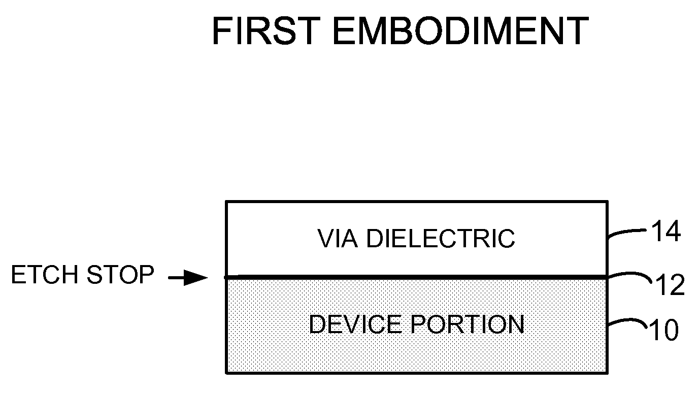
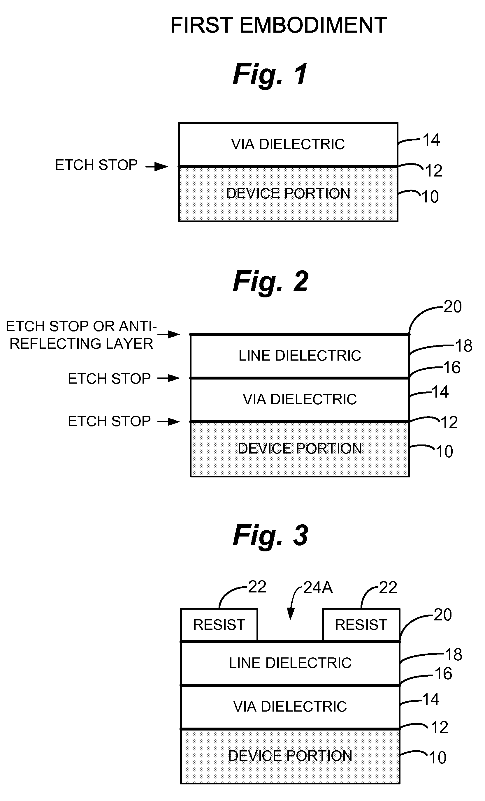
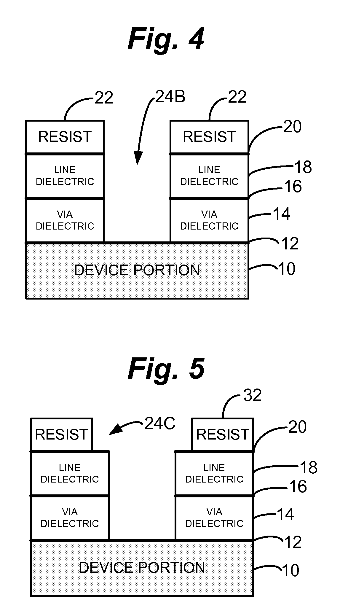
[0028] Referring generally now to FIGS. 1-13, a method for forming an integrated circuit device having an air gap structure is shown for a dual damascene-type metal interconnect structure.
[0029] In FIG. 1, a device layer 10 is formed, which may be a simple silicon substrate and first-level metal, for example. The device layer 10 may nonetheless also include multiple levels of metal, transistors, capacitors, or other devices, including previously manufactured integrated air gap structures built according to the method of the present invention. Thus, device layer 10 is meant to represent that portion of the previously formed integrated circuit device on which the air gap structure is to be built, but it is not limited to any particular form, structure or circuitry.
[0030] Similarly, as used herein, the terms “on” or “onto” or “above” when used in connection with various thin film layers are merely intended to denote a physical spatial relationship, and not necessarily a direct physic...
second embodiment
[0072] Referring generally now to FIGS. 14-24, a method for forming an integrated circuit device having at least one air gap structure is shown for a conventional metal interconnect structure of the type having aluminum alloy metal interconnect layers and tungsten metal plugs. Except where otherwise noted, like numerals are intended to represent like structures and materials already identified in connection with FIGS. 1-13.
[0073] In FIG. 14, a device layer 10 is formed as before.
[0074] A contact / via dielectric layer 14 is formed on device layer 10. As before, dielectric layer 14 is ideally silicon dioxide but can also be USG, FSG, PSG, BPSG, or the like and is deposited to a thickness of about 1000 to 10000 Angstroms. It will be understood, of course, that layer 14 may be comprised of a combination of layers, and formed in more than one processing step, but for purposes of the present discussion, it will be referred to as a single layer.
[0075] In FIG. 15, a photoresist layer 22 i...
third embodiment
[0088] Referring generally now to FIGS. 25-33, a third embodiment of a method for forming an integrated circuit device having at least an air gap structure is shown for a conventional metal interconnect structure of the type having aluminum alloy metal interconnect layers and aluminum alloy metal plugs. The primary difference to the second embodiment is in the use of a different type of a barrier metal layer for the interlayer plugs.
[0089] In FIG. 25, a contact / via dielectric layer 14 is formed on device layer 10 as before.
[0090] In FIG. 26, a photoresist layer 22 is formed and patterned on dielectric layer 14 as before to form a pattern of openings 86A.
[0091] In FIG. 27, openings 86B are etched into contact / via dielectric layer 14 as before.
[0092] In FIG. 28, resist layer 22 is stripped and an aluminum barrier layer 94 (such as Ti / TiN, Ta, TaN or Aluminum oxide) is deposited on the surface of dielectric layer 82 and in openings 86. Again, these are merely examples of those know...
PUM
 Abstract
Description
Claims
Application Information
 - R&D
- Intellectual Property
- Life Sciences
- Materials
- Tech Scout
- Unparalleled Data Quality
- Higher Quality Content
- 60% Fewer Hallucinations
Browse by: Latest US Patents, China's latest patents, Technical Efficacy Thesaurus, Application Domain, Technology Topic, Popular Technical Reports.
© 2025 PatSnap. All rights reserved.Legal|Privacy policy|Modern Slavery Act Transparency Statement|Sitemap|About US| Contact US: help@patsnap.com


