
Systems and methods for writing data with a FIFO interface

a data interface and data technology, applied in the direction of electronic circuit testing, transmission, instruments, etc., can solve the problems of increasing circuit complexity, high degree of mechanical complexity and cost, unsatisfactory results, etc., to improve code portability, reduce on-card i/o counts, and promote commonality

Active Publication Date: 2007-03-29
LIONRA TECH LTD
View PDF47 Cites 16 Cited by
  • Summary
  • Abstract
  • Description
  • Claims
  • Application Information

AI Technical Summary

Benefits of technology

[0010] The disclosed systems and methods may be implemented in a variety of environments including, but not limited to, signal processing applications, communication applications, interfacing applications, networking applications, cognitive computing applications, test and measurement applications, etc. For example, the disclosed systems and methods may be implemented as part of a reconfigurable hardware architecture (“RHA”), such as a reconfigurable signal processing circuit, that serves as a consistent framework in which ASIC applications may be user-defined and / or deployed in such a way as to enhance code portability, design re-use, and intercommunication, as well as to support board-level simulations extending beyond and between individual ASIC boundaries.
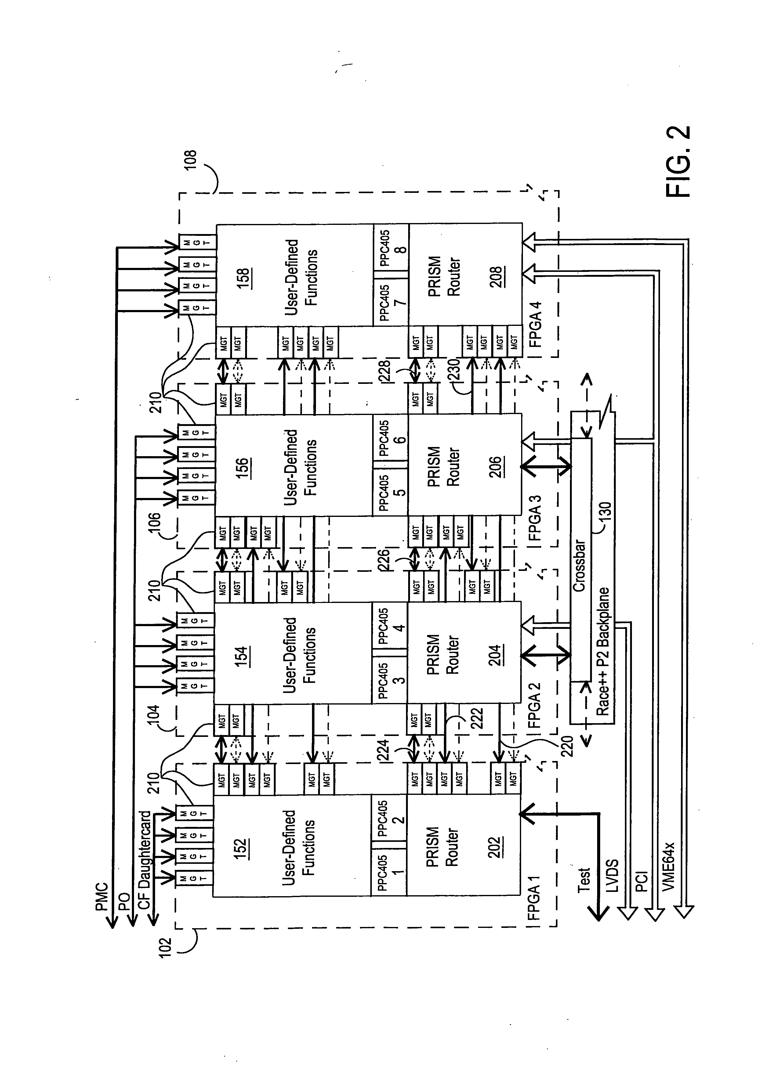
[0011] In one embodiment, a RHA may be configured to include a packet-based communications infrastructure that uses a high-bandwidth switch fabric (e.g., crossbar, etc.) packet router to establish standard communications protocols between multiple interfaces and / or multiple devices that may be present on a single circuit card (e.g., interfaces, processor nodes, and user-defined functions found on signal processing cards). Such a RHA may be further configured in one embodiment to provide a useful communications framework that promotes commonality across multiple (e.g., all) signal processing applications without restricting user utility. For example, packets conforming to a given interface (e.g., Race++ standard) may be processed by stripping the packet header off and then routing the remaining packet between ASIC devices using the standardized packet router infrastructure of the disclosed methods and systems. Advantageously, such a RHA may be implemented in a manner that does not preclude the addition of high-performance user connectivity, e.g., by only using a relatively small fraction of the available serial I / O connections (e.g., MGT connections) and ASIC (e.g., FPGA) gate resources. In one specific embodiment, embedded serial I / O connections (e.g., embedded MGT connections) of multiple FPGA devices may be used to interconnect the FPGA devices in a manner that advantageously reduces on-card I / O counts and the need for large numbers of termination components. However, it will be understood that non-embedded serial I / O connections may also be employed in the practice of the disclosed systems and methods.
[0012] In the practice of one exemplary embodiment of the disclosed systems and methods, multiple FPGAs of a FPGA array may be coupled together on a single card to communicate at the card-level basis using packet routing through one or more switch fabrics, e.g., crossbar switches, etc. In such an embodiment, each given pair of FPGA devices of a FPGA array may be linked in a manner that advantageously minimizes packet transfer latency times in the switch fabric, while at the same time allowing every source to have access to every destination in the array. In such an embodiment, a universal bridging method may be used in each FPGA to allow intercommunication between any two processors / interfaces on a single circuit card. In one exemplary embodiment, the bridging method may be implemented with a First-In First-Out (“FIFO”) packet relay protocol that may be readily integrated into or mapped onto the slave functionality of standard interfaces and / or processor buses.
[0013] Thus, the disclosed systems and methods may be implemented using a predictable and uniform or standardized interface across the boundaries between each pair of board-level components (e.g., FPGAs, ASICs, general-purpose processors, etc.) to help promote consistent communications, board-level testability, design portability / re-use, and to provide a user with a relatively high degree of flexibility in establishing functional partitions for hardware modules mapped into an ASIC (e.g., FPGA) array. Further, built-in support for packet integrity checking and automatic retransmission of bad packets may be provided to facilitate the usage of the inter-ASIC links with hardware modules (e.g., signal processors such as Software-Defined Radios(SDRs), signal processing algorithms such as Fast-Fourier Transforms (FFTs) and wavelet transforms, data stream encryption and decryption, packet routing, etc.) that are sensitive to data corruption. For example, packet integrity checking (e.g., checksum, CRC, etc.) may be incorporated into the hardware layer (e.g., physical layer 1 of Open System Interconnection “OSI” protocol), for example, so that data may be transferred between hardware devices using a packet integrity checking method that is handled automatically by the hardware without the need for an upper layer of software to perform the packet integrity checking. For example, packet integrity protocol tasks (e.g., such as packet acknowledge, timeout, and retransmit tasks) may be built into interface / interconnection hardware present in a data communication link between ASICs or other devices. Using the configuration of the above-described embodiment, a ASIC array may be configured so as to be easily scaleable to other cards, e.g., permitting expansion of ASIC resources. Where described herein in relation to a FPGA array, it will be understood that the disclosed systems and methods may be implemented with an array of any other type of ASIC device or an array of a combination of types such devices.

Problems solved by technology

Such configurations use many wires (along with associated I / O counts and termination components) to achieve required data transfer bandwidths, thus requiring the creation of many connection layers on a circuit card leading to undesirable outcomes such as a high degree of mechanical complexity and cost.
Additional parallel wiring is typically employed when a FPGA array is used to implement multiple card-level interfaces and embedded processor nodes, further increasing circuit complexity.
In addition, diverse types of interfaces (VME64x, Race++, and PCI), processors and user hardware modules are often required to communicate with each other on a single card, further complicating inter-card communications issues.
Banking of I / O pins has reduced the need for termination components, but large I / O counts still require many layers to route, driving printed circuit board (“PCB”) layer counts and costs upward.
However, such JTAG serial interconnections are not suitable for functions such as high-speed data transfer or signal processing.
Thus, the use of multiple large FPGAs, embedded processors, and various standard interfaces on a single card present significant problems with card layout / routing and inter-card communication.

Method used


Image

  • Systems and methods for writing data with a FIFO interface
  • Systems and methods for writing data with a FIFO interface
  • Systems and methods for writing data with a FIFO interface

Examples


Embodiment Construction

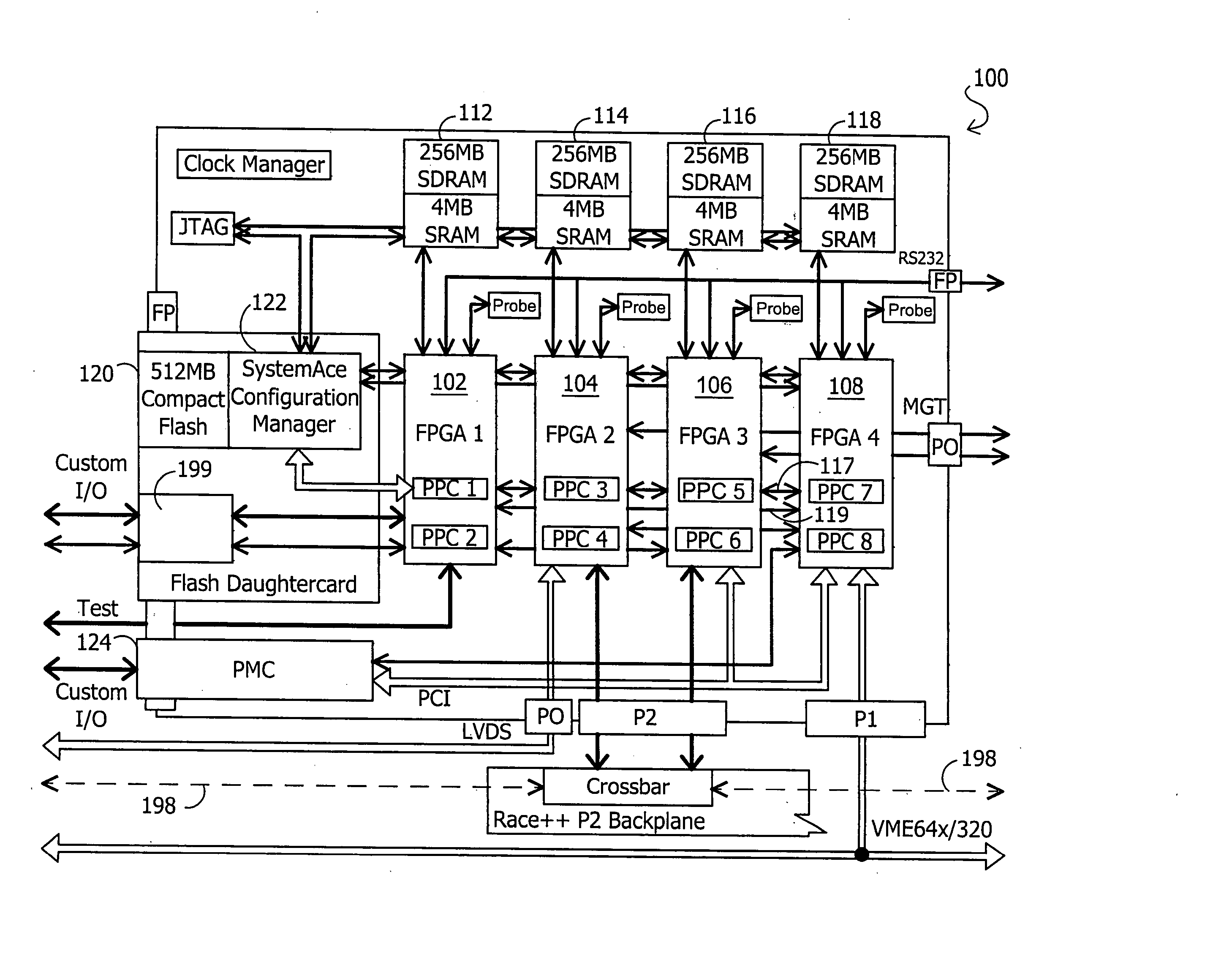
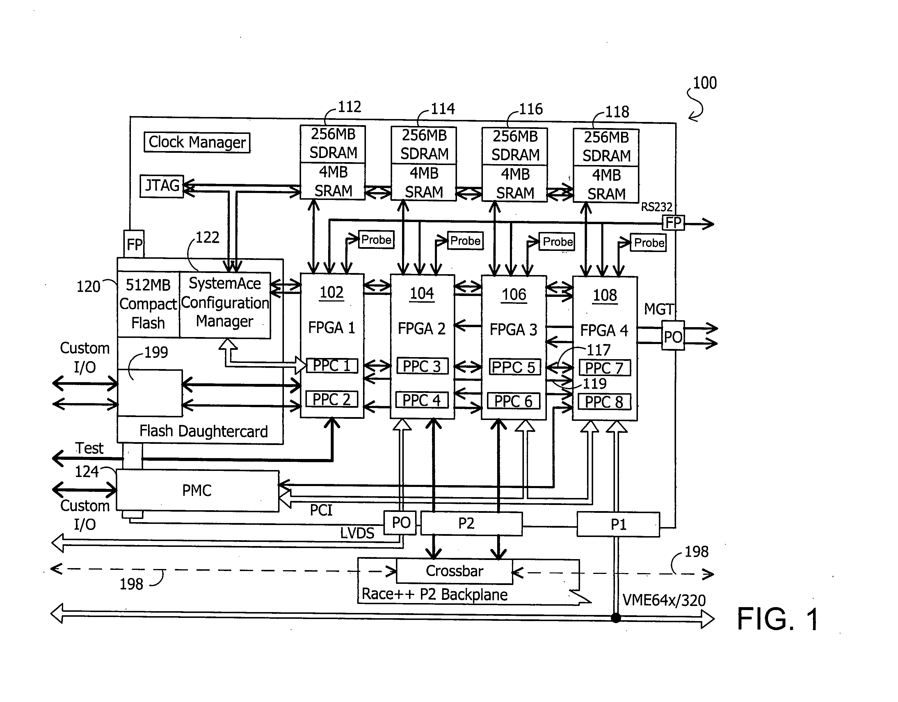
[0032]FIG. 1 illustrates a reconfigurable signal processing circuit 100 as it may be configured on a single circuit card for reconfigurable signal processing and I / O applications according to one exemplary embodiment of the disclosed systems and methods. As shown in FIG. 1, multiple ASIC devices may be provided on a single circuit card, in this exemplary embodiment in the form of four FPGA devices 102, 104, 106 and 108. As will be described further herein, a packet router interface switch matrix (“PRISM”) may be provided to route packets between FPGA devices 102, 104, 106 and 108, and other card-level and off-card devices and interfaces in a manner as will be described further herein. As illustrated in the figures herein, arrowhead notation is provided to indicate signal communication with a particular component. In this regard, an arrowhead that intersects a given device or component indicates signal communication to that given component in the direction indicated, while a line wit...


PUM


Abstract

Application Specific Integrated Circuit (“ASIC”) devices, such as Field Programmable Gate Arrays (“FPGAs”), may be interconnected using serial I / O connections, such as high speed multi-gigabit serial transceiver (“MGT”) connections. For example, serial I / O connections may be employed to interconnect a pair of ASICs to create a high bandwidth, low signal count connection, and in a manner so that any given pair of multiple ASIC devices on a single circuit card may communicate with each other through no more than one serial data communication link connection step. A reconfigurable hardware architecture (“RHA”) may be configured to include a communications infrastructure that uses a high-bandwidth packet router to establish standard communications protocols between multiple interfaces and / or multiple devices that may be present on a single circuit card. Additionally, a communications infrastructure may be established across multiple circuit cards.

Description

[0001] This patent application is a continuation of co-pending U.S. Ser. No. 10 / 843,226, Attorney Docket no. LCOM:011, entitled “Systems And Methods For Interconnection Of Multiple FPGA Devices”, filed on May 11, 2004 which is incorporated herein by reference.BACKGROUND OF THE INVENTION [0002] 1. Field of the Invention [0003] This invention relates generally to interconnection of multiple electrical devices, and more particularly to interconnection of multiple ASIC devices, for example, multiple Field Programmable Gate Array (FPGA) devices. [0004] 2. Description of the Related Art [0005] In the past, multiple FPGA devices have been interconnected as an array on a single circuit card using point-to-point or bussed parallel wiring configurations. Such configurations use many wires (along with associated I / O counts and termination components) to achieve required data transfer bandwidths, thus requiring the creation of many connection layers on a circuit card leading to undesirable outc...

Claims


Application Information

Patent Timeline
Patent Type & Authority Applications(United States)
IPC IPC(8): G06F17/50G06F13/00G06F13/42
CPCG06F13/4256
Inventor YANCEY, JERRY W.KUO, YEA Z.
Owner LIONRA TECH LTD
Learn More