Method of forming carbon-containing silicon nitride layer

Active Publication Date: 2007-03-15
UNITED MICROELECTRONICS CORP
View PDF6 Cites 4 Cited by
  • Summary
  • Abstract
  • Description
  • Claims
  • Application Information

AI Technical Summary

Benefits of technology

[0008] Accordingly, the present invention is directed to a method for forming a carbon-containing silicon nitride layer with superior uniformity, by low pressure chemical vapor deposition (LPCVD) using disilane, ammonia and at least one carbon-source precursor as reactant gases. Moreover, the carbon content of the formed carbon-containing silicon nitride layer can be higher than 9%.
[0009] The present invention is also directed to a method for forming a gate structure, by forming offset spacers or spacers including at least a carbon-containing silicon nitride layer of superior uniformity and high carbon content. Therefore, the performance of the device can be enhanced.
[0012] According to the method for forming the carbon-containing silicon nitride layer proposed in this invention, the carbon-containing silicon nitride layer can offer better superior uniformity and high carbon content, when compared with the conventional silicon nitride layer. Furthermore, the carbon in the resultant silicon nitride layer can help trap free hydrogen in the device and prevent boron diffusion exacerbated by free hydrogen. Therefore, due to less free hydrogen and better uniformity, the electrical characteristics of the device are improved.

Problems solved by technology

As the device dimension shrinks, the channels become shorter, thus inducing undesirable short channel effects.
However, when the size of the device and the line-width shrink, the thickness of each layer and the process margin in each layer also become smaller.
Especially if the offset spacer or spacer is made from a non-uniform silicon nitride layer, not only the junction depth of the subsequent doped regions region may be diverse, the effective channel length of the gate electrode may also be changed, which significantly affects the reliability and uniformity of the semiconductor devices on the wafer.

Method used


Image

  • Method of forming carbon-containing silicon nitride layer
  • Method of forming carbon-containing silicon nitride layer
  • Method of forming carbon-containing silicon nitride layer

Examples


Embodiment Construction

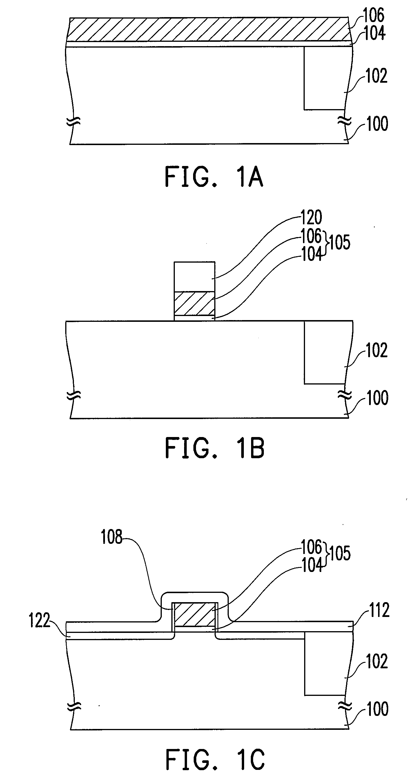
[0016] Reference will now be made in detail to the present preferred embodiments of the invention, examples of which are illustrated in the accompanying drawings. Wherever possible, the same reference numbers are used in the drawings and the description to refer to the same or like parts.

[0017] As mentioned above, as the line-width minimizes and the thickness of each layer shrinks, it is important to enhance the uniformity of certain layers, such as the silicon nitride layer for the offset spacer or the spacer for better-quality device or improved standardization of the devices within the wafer.

[0018] Currently, it is common to employ SiH4 and NH3 as the reactant gases for forming the silicon nitride layer by the single wafer tools. However, the obtained silicon nitride layer has inferior and unsatisfactory within wafer uniformity, wafer-to-wafer uniformity and lot-to-lot uniformity. Alternatively, furnace can be used to form the silicon nitride layer for the wafers in batch. Howe...


PUM

PropertyMeasurementUnit
Fractionaaaaaaaaaa
Fractionaaaaaaaaaa
Fractionaaaaaaaaaa

Abstract

A method for forming a carbon-containing silicon nitride layer with superior uniformity by low pressure chemical vapor deposition (LPCVD) using disilane, ammonia and at least one carbon-source precursor as reactant gases is provided.

Description

CROSS-REFERENCE TO RELATED APPLICATION [0001] This application claims the priority benefits of U.S. provisional application serial No. 60 / 716,848, filed on Sep. 13, 2005. All disclosure of this application is incorporated herein by reference.BACKGROUND OF THE INVENTION [0002] 1. Field of the Invention [0003] The present invention generally relates to a method of forming a semiconductor device. More particularly, the present invention relates to a method for forming a carbon-containing silicon nitride layer. [0004] 2. Description of Related Art [0005] The metal-oxide-semiconductor (MOS) field effect transistor is the most important device applied for ultra-large-integrated-circuits, such as microprocessors and semiconductor memories. The MOSFET transistor generally includes a conductive gate structure and a source / drain region disposed on both sides of the gate structure. To increase the number of components per IC chip, the device dimensions must be scaled down. As the device dimens...

Claims


Application Information

Patent Timeline
IPC IPC(8): H01L21/338H01L21/00
CPCC23C16/36H01L21/3185H01L29/7833H01L29/6659H01L29/6656H01L21/02167H01L21/02216H01L21/0228H01L21/02211H01L21/02271
Inventor CHENG, PO-LUN
Owner UNITED MICROELECTRONICS CORP
Why Eureka
Try Eureka