Process for modifying dielectric materials
a dielectric material and dielectric technology, applied in the direction of semiconductor/solid-state device manufacturing, electric devices, basic electric elements, etc., can solve the problems of inherently weaker low-k dielectric materials, affecting the mechanical strength of low-k dielectrics and silicon-level interconnects compared to previous-generation materials, and affecting the downstream electronic-packaging process and materials. , to achieve the effect of restoring the hydrophobicity of the surface and increasing the hydrophobicity
- Summary
- Abstract
- Description
- Claims
- Application Information
AI Technical Summary
Benefits of technology
Problems solved by technology
Method used
Image
Examples
example 1
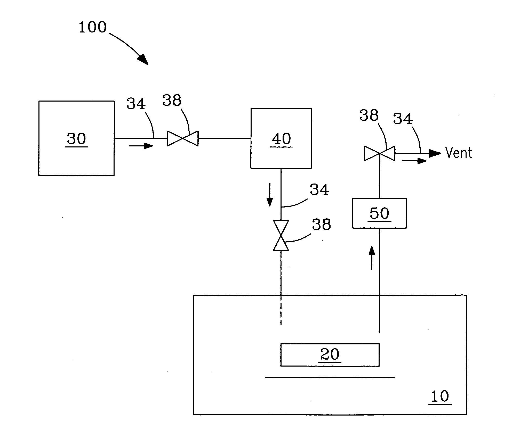
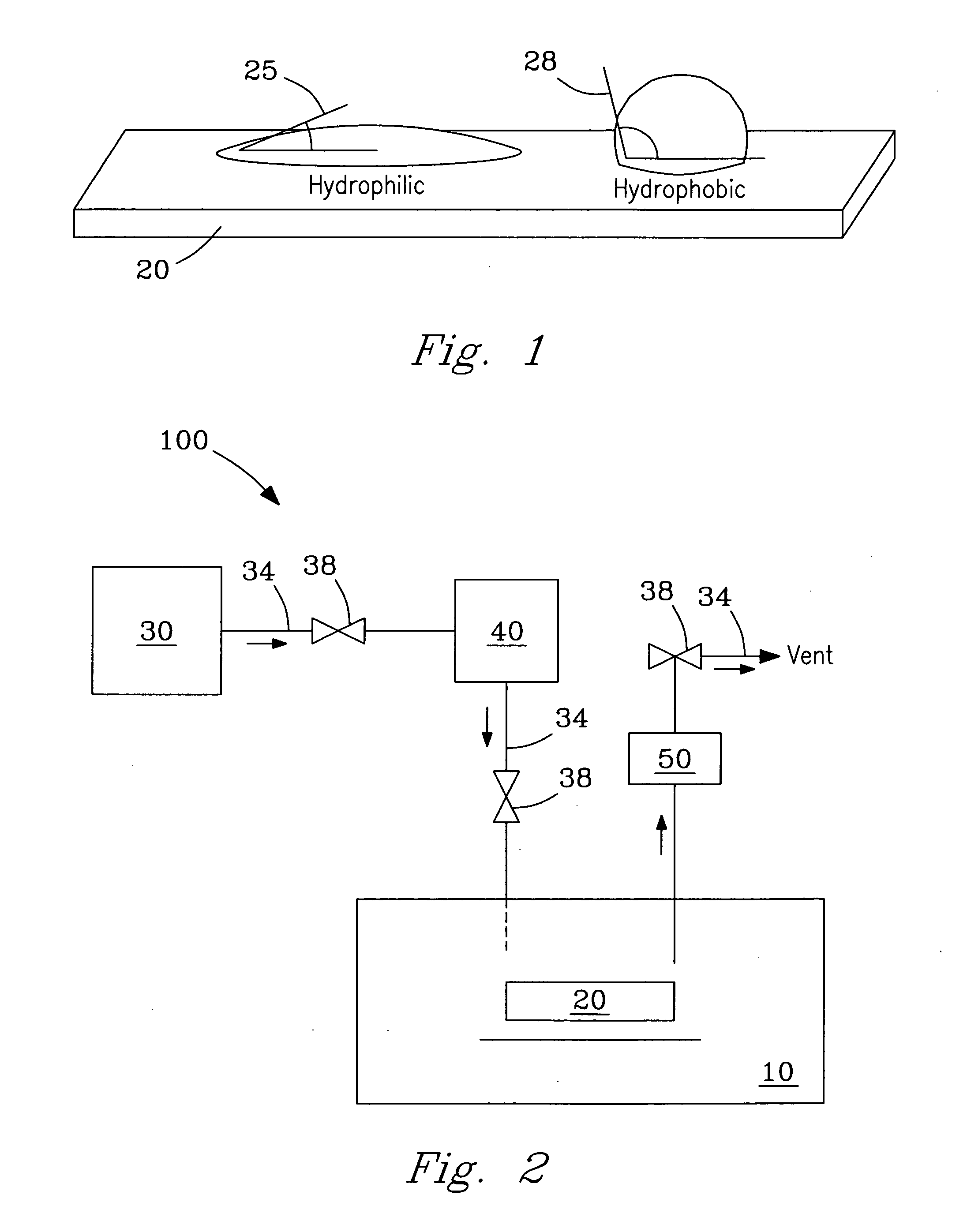
[0056] Example 1 describes repair of dielectric substrates 20 treated using an alkoxysilane reagent (e.g., n-PTMS) as a function of reactor 10 temperature. Modifier reagents including water and acetic acid were optionally added to initiate, promote, and / or catalyze polymerization and / or cross-linking of the silylating reagent. In exemplary tests, premixing vessel 40 was charged with ˜5 μL of reagent grade n-propyltrimethoxysilane (n-PTMS) (Gelest, Inc., Philadelphia, Pa.) and 10 μL H2O. Reactor 10 was pressurized with solvent fluid comprising carbon dioxide to a pressure of 2500 psig achieving a concentration for the n-PTMS reagent in the near-critical or supercritical solvent fluid (reagent fluid) of about 0.01 wt %, but is not limited thereto. In other tests, substrates 20 were subjected to n-PTMS reagent (mixed in the solvent fluid) further comprising various modifiers (equal weight percentage). In other tests, substrates 20 were subjected to an optional pre-clean step, as descri...
example 2
[0058] Example 2 presents results for n-PTMS repair of damaged dielectric substrates in conjunction with use of a low-temperature repair and a high-temperature “bake” (cure), according to another embodiment of the invention. A dielectric substrate 20 damaged by, e.g., etch processing was introduced to reactor 10. Premixing vessel 40 was charged with ˜5 μL of reagent grade n-propyltrimethoxysilane (n-PTMS) (Gelest, Inc., Philadelphia, Pa.) and 10 μL H2O to initiate polymerization and / or cross-linking of the n-PTMS reagent. Reactor 10 was pressurized with solvent fluid comprising carbon dioxide to a pressure of 2500 psig achieving a concentration for the n-PTMS reagent in the near-critical or supercritical solvent fluid of about 0.01 wt %, but is not limited thereto. A low operating temperature of reactor 10 for repair was selected in the range from about 25° C. to about 40° C., but is not limited thereto. In exemplary tests, substrates 20 were treated with n-PTMS at a (deposition) te...
example 3
[0060] Example 3 presents n-PTMS repair results for damaged dielectric substrates subjected to an initial pre-clean step. In exemplary tests, pre-clean solution was a dilute (1:1000) HF solution (HF:H2O) prepared in deionized water. Substrates were immersed in the HF solution for about 60 seconds, rinsed in deionized water, and dried under nitrogen gas stream for about 60 seconds. In alternate tests, pre-clean solution was a surfactant solution, as described in co-pending application Ser. No. 10 / 851,380. State of repair was assessed by exposing substrates repaired in conjunction with n-PTMS to an HF etching (1:100 HF:H2O) solution (“HF Dip”) for 60 seconds, rinsing in deionized water, and drying under nitrogen atmosphere. Evidence of etching and / or degree of etching was indicative of no repair or partial repair. Absence of etching was indicative of complete repair. Table 3 presents HF etch (“HF Dip”) test results (nm) listing average critical dimension changes measured for sets of f...
PUM
| Property | Measurement | Unit |
|---|---|---|
| Young's modulus | aaaaa | aaaaa |
| interfacial contact angle | aaaaa | aaaaa |
| temperature | aaaaa | aaaaa |
Abstract
Description
Claims
Application Information
 - R&D
- Intellectual Property
- Life Sciences
- Materials
- Tech Scout
- Unparalleled Data Quality
- Higher Quality Content
- 60% Fewer Hallucinations
Browse by: Latest US Patents, China's latest patents, Technical Efficacy Thesaurus, Application Domain, Technology Topic, Popular Technical Reports.
© 2025 PatSnap. All rights reserved.Legal|Privacy policy|Modern Slavery Act Transparency Statement|Sitemap|About US| Contact US: help@patsnap.com


