
Channel discharging after erasing flash memory devices

a flash memory device and channel discharge technology, applied in semiconductor devices, digital storage, instruments, etc., can solve problems such as device latchup, and achieve the effect of relaxing any demand on high voltage supply and shortening supply of high capacity

Active Publication Date: 2007-02-01
ARTEMIS ACQUISITION
View PDF19 Cites 3 Cited by
  • Summary
  • Abstract
  • Description
  • Claims
  • Application Information

AI Technical Summary

Problems solved by technology

In memory devices having a P-well within a deep N-well, the channel clearing operation after an erase can present a special challenge.
Forward bias on a vertical parasitic junction can cause device latchup.

Method used


Image

  • Channel discharging after erasing flash memory devices
  • Channel discharging after erasing flash memory devices
  • Channel discharging after erasing flash memory devices

Examples


Embodiment Construction

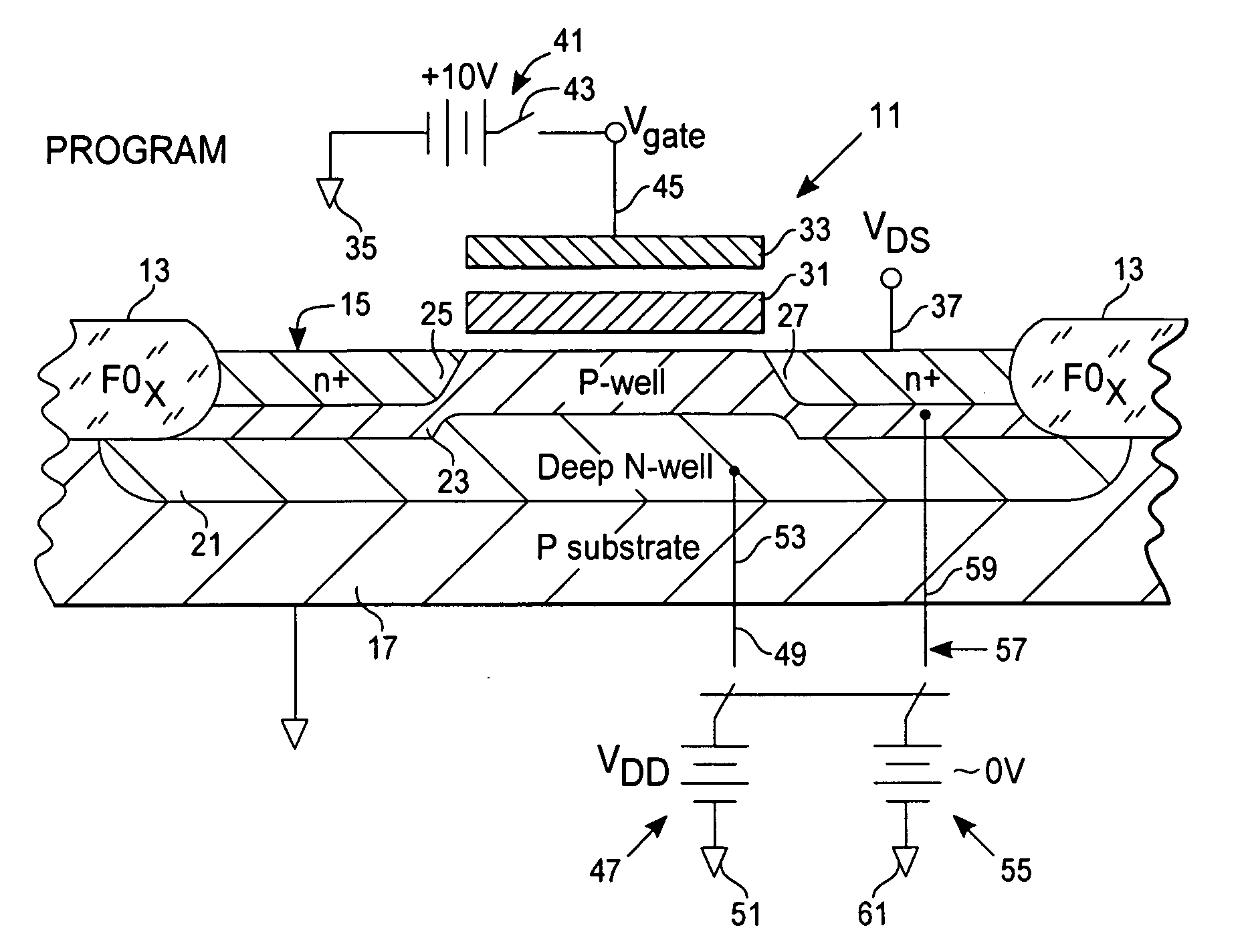
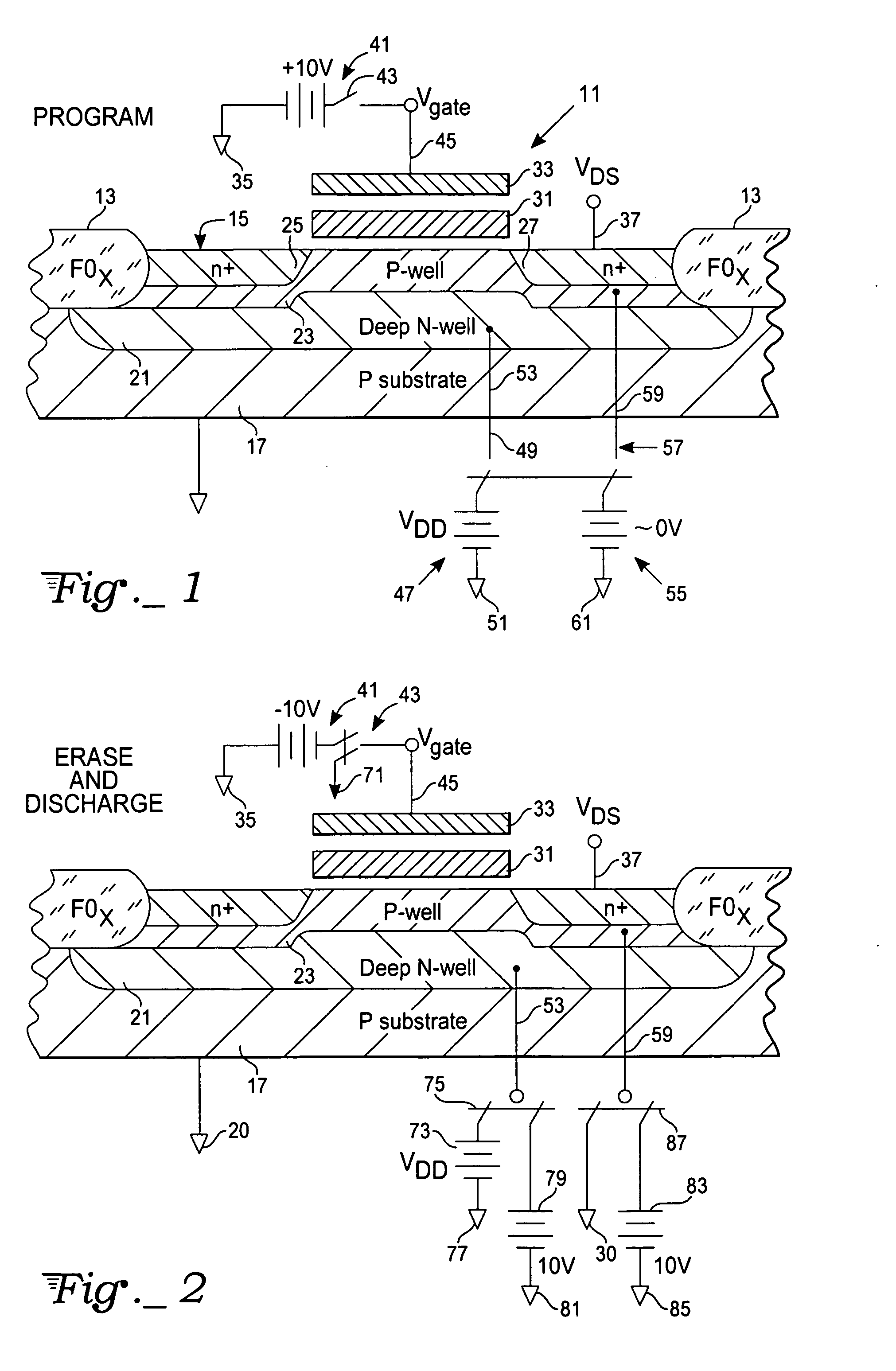
[0011] With reference to FIG. 1, a non-volatile memory cell 11, typically an EEPROM (electrically erasable programmable read only memory) transistor, is constructed within a silicon wafer or substrate 17, shown as a p-type substrate. Within this substrate the memory cell 11, an EEPROM device, is built within an active region defined by a field oxide boundary 13. The substrate has a surface 15, with portions of the device above the surface and portions below.

[0012] Below surface 15, a deep N-well 21 is established in substrate 17, overlapping with the field oxide boundaries 13 across the entire subsurface regions of the device, by implantation or diffusion of n-type ionic impurities in a known manner. After N-well 21 is established a less deep P-well 23 is established within the upper half, more or less, of the deep N-well 21. The P-well 23 extends from surface 15 downwardly to about one-half of the depth of the N-well 21 and from one field oxide boundary to the other. Building of a...


PUM


Abstract

A post-erase channel clearing procedure for double well, floating gate, non-volatile memory cells. The channel is cleared of charged particles coming from the floating gate after an erase operation in two steps. In the first step the charged particles are pushed into an upper substrate well below the floating gate but not allowed into a deeper well of opposite conductivity type relative to the upper well. After a brief time, T, the charged particles are pushed by a bias voltage into the deeper well from the upper well. This two step clearing procedure avoids device latchup that might occur otherwise.

Description

TECHNICAL FIELD [0001] The invention relates to non-volatile memory transistors and, in particular, to a post-erase channel clearing procedure for double well non-volatile memory transistors in a flash array memory architecture. BACKGROUND ART [0002] Well voltage control after an erase operation in non-volatile memory transistors is important for preventing latchup, a condition that prevents useful operation. Generally, latchup occurs due to the presence of parasitic PN junctions, particularly when the junctions form parasitic NPN and PNP bipolar transistors. Typically a parasitic transistor is a vertical transistor formed in subsurface wells. When two parasitic transistors interact, the second one often a lateral transistor, latchup occurs. An anti-latchup invention is described in U.S. Pat. No. 6,549,465 to Y. Hirano et al. In the patent, a well voltage setting circuit has a P-MOS transistor for applying an erase pulse, a first N-MOS transistor for applying a reference voltage Vss...

Claims


Application Information

Patent Timeline
Patent Type & Authority Applications(United States)
IPC IPC(8): G11C16/04
CPCH01L29/7883G11C16/14
Inventor TRINH, STEPHEN T.
Owner ARTEMIS ACQUISITION
Learn More