Semiconductive film, electric charge control member and process for production the semiconductive film

Inactive Publication Date: 2007-01-25
KUREHA KAGAKU KOGYO KK
View PDF5 Cites 16 Cited by
  • Summary
  • Abstract
  • Description
  • Claims
  • Application Information

AI Technical Summary

Benefits of technology

[0025] It is an object of the present invention to provide a semiconductive film that is formed from a resin composition comprising poly(ether ether ketone) and a conductive filler, narrow in scatters of both thickness and volume resistivity and markedly excellent in folding endurance (flexing resistance), and a production process thereof.
[0027] A further object of the present invention is to provide a charge controlling member such as a belt or covered roller formed from the above-described semiconductive film having excellent properties.

Problems solved by technology

For example, if a charging belt wide in the scatter of volume resistivity is used, it is impossible to evenly charge the surface of the photosensitive body.
If a transfer belt wide in the scatter of volume resistivity is used, it is impossible to exactly transfer the toner image on the surface of the photosensitive body to a transfer material.
As a result, it is impossible to obtain an high-quality image.
For example, if the modulus in tension of a belt is too low, the belt is distorted, so that the durability of the belt itself is impaired, and moreover in the case of an intermediate transfer belt, it forms the cause of distortion and color drift of a toner image transferred on the belt.
If the tensile elongation at break of a charge controlling member is too low, its flexibility becomes insufficient, so that its breakage by entrainment of foreign matter, or the like is easy to occur.
Since the charge controlling members are often used in a high-temperature atmosphere, and high voltage of 100 V to several kV or higher may be applied to charge controlling members and the like installed in an electrophotographic copying machine in some cases, they are exposed to the risk of firing by sparks or heating.
However, this film is wide in a scatter of volume resistivity with location and hard to be subjected to incineration disposal after use.
A film formed from a resin composition obtained by dispersing conductive carbon black in a thermoplastic polyester resin involves a problem that creep at 70° C. is high, in addition to the fact that it is wide in a scatter of volume resistivity with location.
A belt too high in the creep tends to deform attending on the form of a driving roller and cause image failure by the distortion of the belt.
However, many of polyimide resins are difficult to be subjected to melt extrusion, so that it is necessary to form a film, belt or the like by a wet forming method making use of a varnish containing a polyimide precursor, and so vast production cost is required.
However, it has been extremely difficult to produce a semiconductive film, which has an even thickness and is narrow in a scatter of volume resistivity with location and excellent in mechanical strength, using a resin composition with a conductive filler added to PEEK.
When the resin composition with the conductive filler added to PEEK is used to form a non-crystalline sheet, and the non-crystalline sheet is biaxially stretched, however, the sheet is broken upon the stretching, so that it is extremely difficult to produce a satisfactory biaxially stretched film.
When a resin composition with a conductive filler dispersed in PEEK is used to produce a semiconductive film by the drawdown method, however, it is difficult to control the thickness of the resulting semiconductive film evenly, and moreover the semiconductive film tends to be easily tore in its flowing direction.
Further, according to this method, the volume resistivity of the resulting semiconductive film is liable to be uneven due to molecular orientation of PEEK.
However, it is difficult to obtain a semiconductive film having an even thickness under such film-forming conditions.
The resultant semiconductive film also tends to be tore in its flowing direction.
However, it is difficult to control so as to give an even thickness even according to this process, and the resultant semiconductive film is wide in a scatter in volume resistivity with location and tends to be tore in its flowing direction.

Method used


Image

  • Semiconductive film, electric charge control member and process for production the semiconductive film
  • Semiconductive film, electric charge control member and process for production the semiconductive film
  • Semiconductive film, electric charge control member and process for production the semiconductive film

Examples


example 1

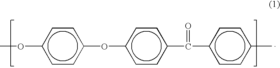
[0106] In a Henschel mixer, 94.0 parts by weight of poly(ether ether ketone) (product of Victrex Co., trade name “Victrex PEEK 450G”) and 6.4 parts by weight of conductive carbon black (oil furnace black, product of Ketjen Black International, trade name “Ketjen Black EC”, volatile matter=0.5%, DBP oil absorption=360 ml / 100 g, pH=9) were uniformly dry-blended. The resultant blend was then fed to a twin-screw kneader extruder (PCM-46, manufactured by Ikegai Corp.) having a barrel diameter of 45 mm, kneaded at a cylinder temperature of 260 to 385° C., and melted and extruded, thereby forming pellets.

[0107] The thus-formed pellets were fed to a singly-screw extruder and melt-extruded in the form of a film from a T type die (T-die) having a lip clearance of 0.5 mm at a die temperature (resin temperature) of 390° C., and the film in the molten state was then brought into contact with a cooling roll controlled to a temperature of 85° C. to produce a film having a thickness of about 50 μm...


PUM

PropertyMeasurementUnit
Temperatureaaaaaaaaaa

Abstract

A semiconductive film formed from a resin composition comprising poly(ether ether ketone) and a conductive filler, wherein the average value of its thickness is 30 to 250 μm, the maximum value of the thickness is 1 to 1.3 times as much as the minimum value thereof, the average value of its volume resistivity is 1.0×10² to 1.0×10¹⁴ Ωcm, the maximum value of the volume resistivity is 1 to 30 times as much as the minimum value thereof, and the number of reciprocating folds as determined in accordance with the testing method for folding endurance is at least 5,000 times, and a production process thereof.

Description

TECHNICAL FIELD [0001] The present invention relates to a semiconductive film formed from a resin composition comprising poly(ether ether ketone) (hereinafter abbreviated as “PEEK”) and a conductive filler and a production process thereof. The present invention also relates to a charge controlling member formed with this semiconductive film. The semiconductive film according to the present invention is suitable for use in charge control members such as charging belts and transfer belts in image forming apparatus of an electrophotographic system or electrostatic recording system. BACKGROUND ART [0002] Synthetic resin films having a volume resistivity within a semiconductive range are used in various fields as raw materials of charge controlling members. Typical technical fields, in which the charge controlling members are used, include image forming apparatus such as copying machines, laser beam printers and facsimiles of an electrophotographic system (including an electrostatic reco...

Claims


Application Information

Patent Timeline
IPC IPC(8): G11B11/105C04B35/00G03G15/00B29C48/08B29C48/10B29C48/305B29C48/32B29K71/00B29K105/16B32B27/08C08J5/18C08K3/00C08L71/10G03G15/02G03G15/16
CPCB29C47/0004B29C47/0021B29C47/14B29C47/20Y10T428/26B29K2071/00B29K2079/08B32B27/08B29C47/8815B29C48/022B29C48/08B29C48/10B29C48/305B29C48/32B29C48/911B29C48/914B29C48/917B32B27/285B32B2371/00B32B27/20
Inventor KITAMURA, HIDEKITERAMOTO, YOSHIKICHISUZUKI, KAZUYUKINISHIHATA, NAOMITSUSUZUKI, YASUHIRO
Owner KUREHA KAGAKU KOGYO KK
Why Eureka
Try Eureka