
Semiconductor integrated circuit device and wireless communication system

a technology of integrated circuits and semiconductors, applied in the field of wireless communication technology, can solve the problems of increasing transmission signal distortion, deteriorating acpr (leak power ratio to the adjacent channel), and increasing signal distortion, so as to achieve the effect of lowering current consumption

Inactive Publication Date: 2006-12-28
IRIE KIYOSHI +2
View PDF7 Cites 6 Cited by
  • Summary
  • Abstract
  • Description
  • Claims
  • Application Information

AI Technical Summary

Benefits of technology

"The patent text describes a problem in the transmission system of a mobile phone in the W-CDMA system. When multiple signals are transmitted simultaneously, the peak factor (the difference between the maximum power and the average output level) increases, causing distortion and degraded performance. The inventors have designed an amplifying circuit with a wider dynamic range to avoid distortion and improve performance. The invention aims to solve this problem in a mobile phone while reducing current consumption and extending battery life."

Problems solved by technology

In the specification of the mobile telephone of the W-CDMA system, it is specified that the data of six channels in maximum can be transmitted from one channel through the multiplexing, but this method has problems that the more the number of multiplexes of data is increased, the more the distortion of transmission signal increases and thereby the ACPR (leak power ratio to the adjacent channel) characteristic is deteriorated.
Moreover, it has been found when the transmission signal is amplified with an amplifying circuit having a narrower dynamic range with the peak factor which is large as described above, distortion of signal increases and the ACPR characteristic is deteriorated.
However, since power consumption of the total system increases when the current of the amplifying circuit increases, it is a problem to be eliminated as much as possible in the system such as a mobile telephone which is operated with a battery.
However, in the mobile telephone of the W-CDMA system, since the transmitting operation and receiving operation are executed simultaneously and continuously, current consumption is considerably larger than that of the mobile telephone of the PDC system.
Therefore, increase in current of the amplifying circuit in the mobile telephone of the W-CDMA system will result in the problem that the maximum communication time and the maximum waiting time which are intrinsically short may be further shortened.

Method used


Image

  • Semiconductor integrated circuit device and wireless communication system
  • Semiconductor integrated circuit device and wireless communication system
  • Semiconductor integrated circuit device and wireless communication system

Examples


second embodiment

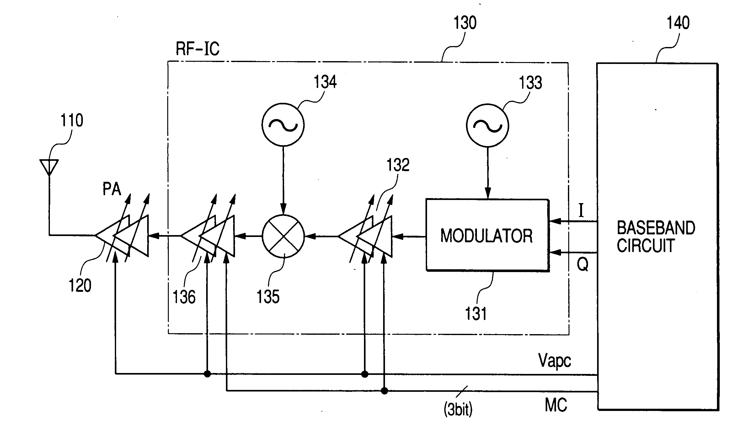
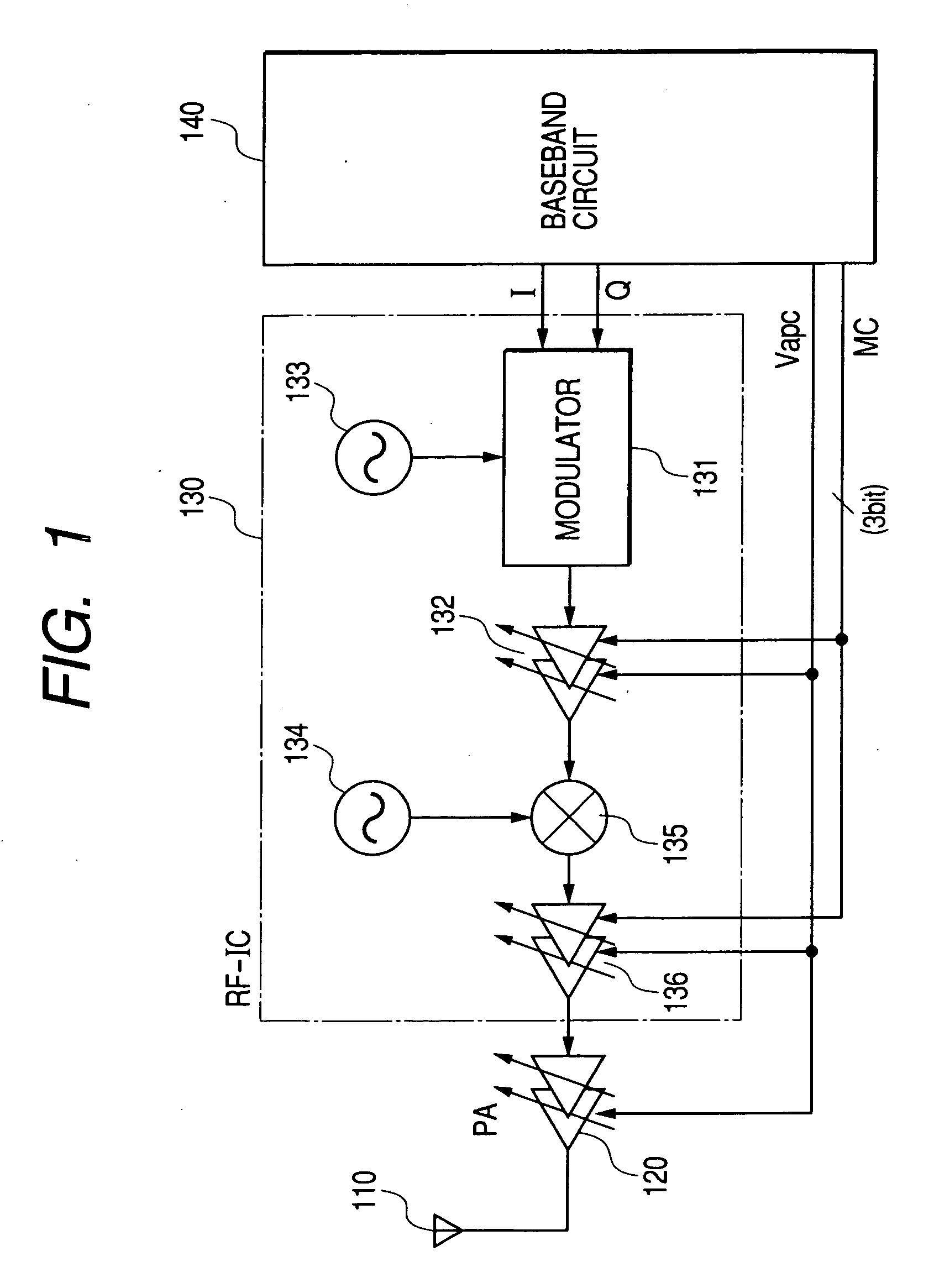
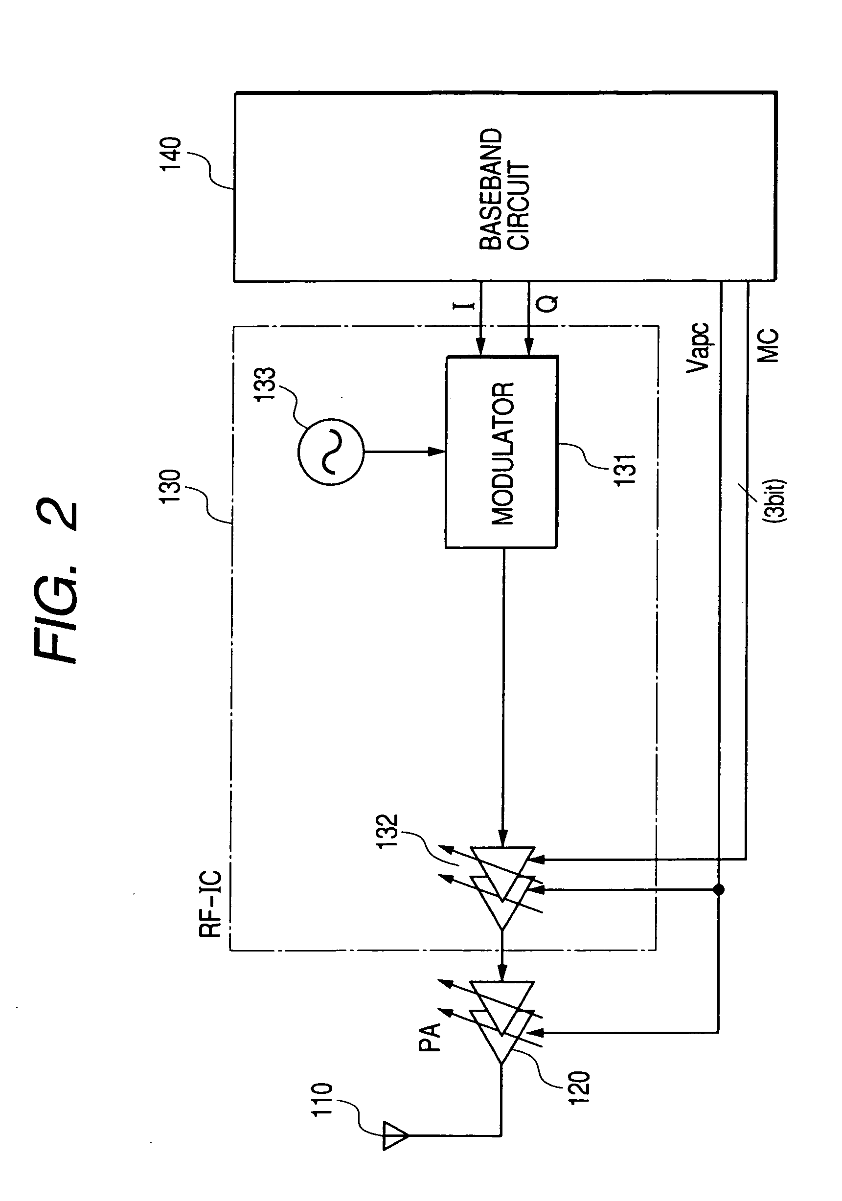
[0055] Moreover, in this second embodiment, the average output levels of the variable gain amplifying portion 132 and power module 120 is adjusted depending on the gain control signal Vapc from the baseband circuit 140, the control information MC indicating the number of code division multiplexes is supplied to the transmission circuit 130 from the baseband circuit 140, and the operation current of the variable gain amplifying portion 132 is switched depending on the control information MC. Even in this embodiment, the control information MC indicating the number of multiplexes may be any one of the 3-bit code or the control voltage of seven voltage levels.

[0056]FIG. 3 and FIG. 4 illustrates a third embodiment when the present invention is applied to the code division multiplex transmission circuit of the mobile telephone of the W-CDMA system. This embodiment is different from the first embodiment only in the method of applying the control information MC indicating the code division...

third embodiment

[0057] In more practical, the transmission circuit 130 of the third embodiment is provided with a mode control circuit 137 which controls the interior of the RF-IC chip such as power ON / OFF of the transmission circuit and setting of frequency of the local oscillators 133, 134 depending on the mode control signal for designating each operation mode supplied from the baseband circuit 140. The mode control circuit 137 and the baseband circuit 140 are connected with three signal lines. One of the three signal lines is a signal line to supply the clock signal CLK, another signal line is used for serial transfer of the data DATA and the remaining signal line is used to supply the load enable signal LE which allows fetching of the data.

[0058] The mode control circuit 137 of this embodiment is provided, although not particularly restricted, with a 10-bit shift register and a 10-bit control register. The serial data DATA is fetched by the shift resistor and is then shifted in synchronization...


PUM


Abstract

The dynamic range is changed by switching a current applied to an amplifying circuit to obtain the minimum ICP required to keep linearity with the number of multiplexes even when the number of multiplexes of data is changed by switching the operation current of the amplifying circuits of the transmission system and also supplying the information about number of multiplexes of data to be transmitted to the amplifying circuits of the transmission system from the baseband circuit. Thereby, the signal can be transmitted without distortion even when the number of multiplexes increases and the current of the amplifying circuit may be reduced when the number of multiplexes is small in order to reduce the current consumption in the communication semiconductor integrated circuit device which can form a wireless communication system of the code division multiplex system such as W-CDMA system.

Description

[0001] The present application is a continuation of application Ser. No. 10 / 685,481, filed Oct. 16, 2003, the contents of which are incorporated herein by reference.BACKGROUND OF THE INVENTION [0002] The present invention relates to a wireless communication technology, more specifically to a technology which may be effectively applied, while increase of power consumption is controlled, for improving linearity of a semiconductor integrated circuit device comprising an amplifying circuit to amplify the code division multiplexed transmitting signal. Moreover, the present invention relates to a technology which may be effectively applied to a semiconductor integrated circuit device for communication constituting a wireless communication device, for example, of W-CDMA (Wideband Code Division Multiple Access) system and to a wireless communication device such as a mobile telephone or the like comprising the same semiconductor integrated circuit device. [0003] In the wireless communication...

Claims


Application Information

Patent Timeline
Patent Type & Authority Applications(United States)
IPC IPC(8): H01Q11/12H04B1/06H04B1/04H03G3/30H03F3/45H03G1/00H04J13/00
CPCH03F3/45098H03F2200/294H03F2203/45496H03F2203/45504H04B2201/70706H03G1/0023H03G1/0088H04B1/707H03F2203/45722
Inventor IRIE, KIYOSHIHORI, KAZUAKIHIKASA, KAZUHIKO
Owner IRIE KIYOSHI
Learn More