
Method for growing silicon single crystal and method for manufacturing silicon wafer

a single crystal and silicon technology, applied in the direction of crystal growth process polycrystalline material growth, etc., can solve the problem that the extent of the pulling rate margin of the defect-free crystal is still insufficient to grow silicon, and the adverse effect of device characteristics may be exerted, so as to achieve the effect of sufficient gettering capability

Active Publication Date: 2006-12-21
SUMCO CORP
View PDF5 Cites 9 Cited by
  • Summary
  • Abstract
  • Description
  • Claims
  • Application Information

AI Technical Summary

Benefits of technology

The present invention relates to a method for growing silicon single crystals with controlled oxygen concentration using a mixed gas containing hydrogen atoms. The method involves controlling the temperature and the ratio of the axial thermal gradient to achieve a desired oxygen concentration. The resulting silicon single crystals have a high pulling rate margin and can be used to manufacture silicon wafers with reduced occurrence of defects. The method also allows for the control of the hydrogen concentration in the silicon single crystal to avoid the formation of oxide precipitates. The resulting silicon wafers have a low oxygen concentration and can be used in various applications.

Problems solved by technology

It is well known that silicon single crystals manufactured by the CZ method include fine defects called grown-in defects.
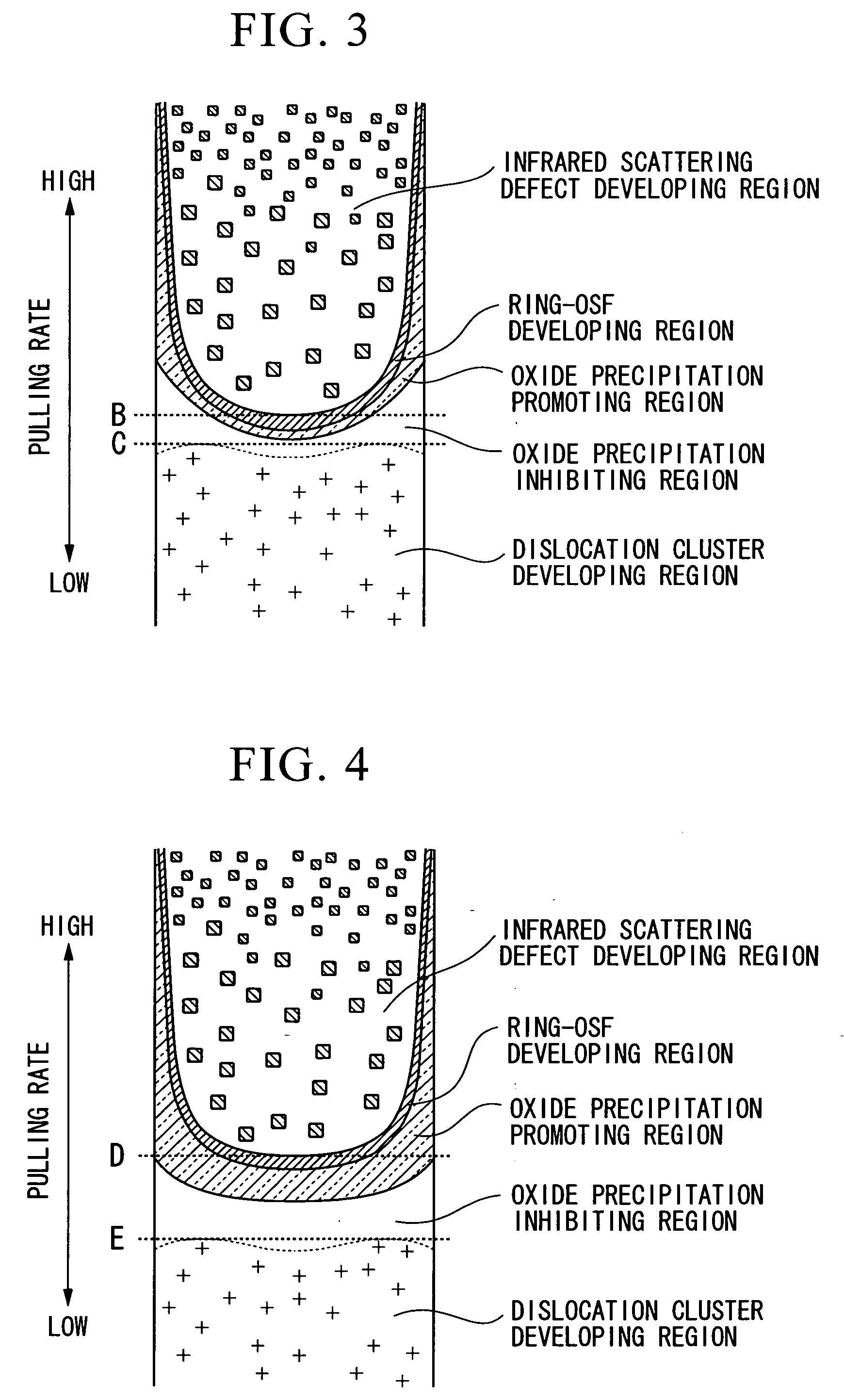
However, even when the pulling rate margin of the defect-free crystal is increased by introducing hydrogen into the pulling furnace as described in Patent Document 1, the extent of the pulling rate margin of the defect-free crystal is still insufficient to grow a silicon single crystal comprising one region selected from among the OSF developing region, the PV region, and the PI region.
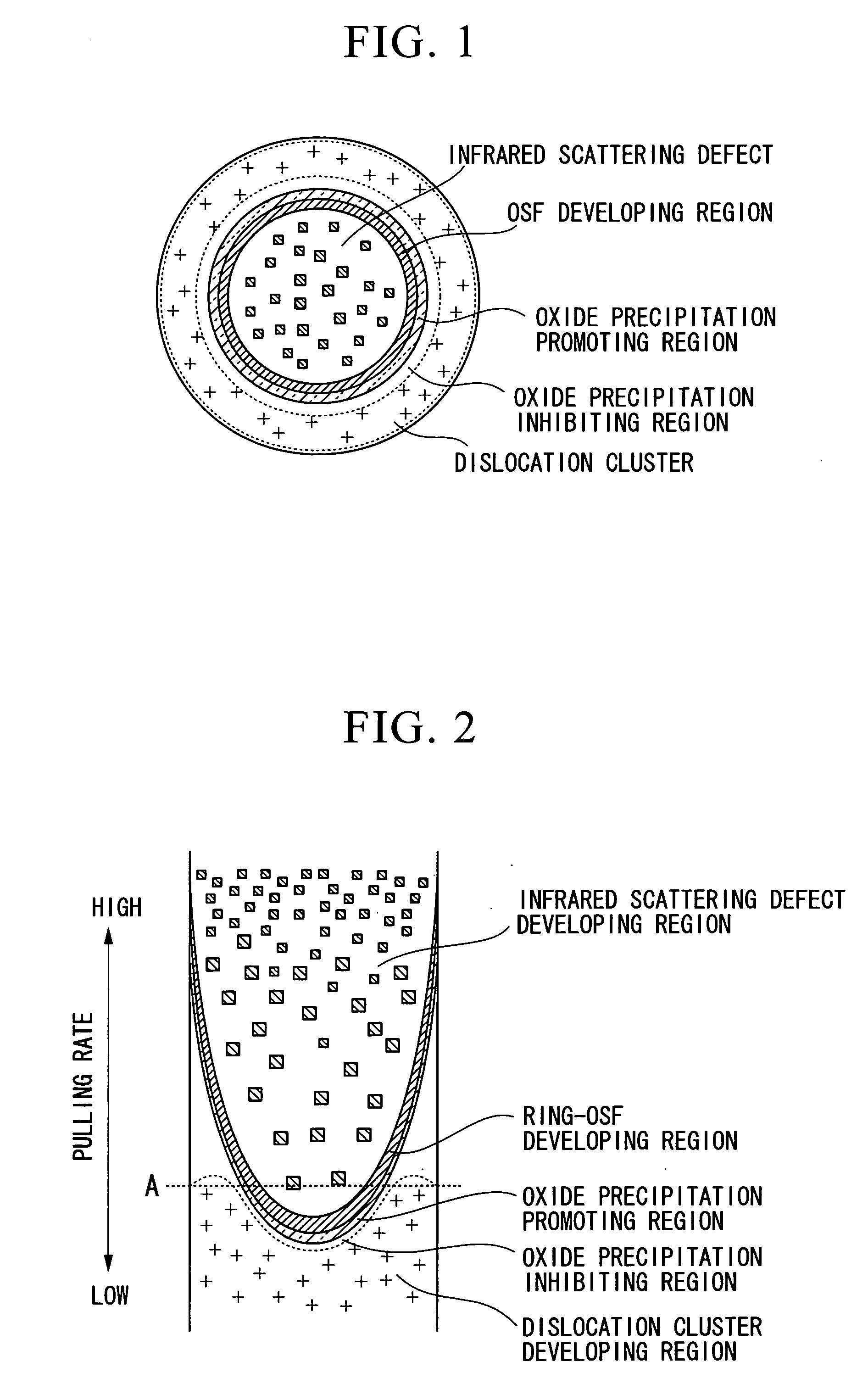
As described above, the OSF developing region is the defect-free region where neither infrared scattering defects nor dislocation clusters are detected; however, when the concentration of oxygen is high, an adverse effect may be exerted on device characteristics because occurrence of OSFs as secondary defects of oxide precipitates becomes apparent.
However, when the oxygen concentration of a silicon single crystal is controlled to have low value not more than 12×1017 atoms / cm3 (ASTM-F121 1979), such a single crystal may not provide a silicon wafer having sufficient density of oxide precipitates to allow a sufficient gettering capability.
In addition, although an active region near a device surface must be free of not only infrared scattering defects and dislocation clusters, but also oxide precipitates and their secondary defects such as OSFs and punch out dislocations, the width of a region free of such defects, that is, DZ width cannot be uniform in a wafer including both PV region and PI region.
The non-uniform distributions of the gettering capability (IG capability) and the DZ width result in variations in device characteristics and a decrease in the yield of device production.
However, since such a growing condition further reduce the narrow range of the pulling rate margin of a defect-free crystal including the OSF developing region, the PV region, and the PI region, stable manufacture of a defect free crystal comprising only one region selected from the OSF developing region, the PV region, and the PI region has been difficult in terms of industrial production.

Method used


Image

  • Method for growing silicon single crystal and method for manufacturing silicon wafer
  • Method for growing silicon single crystal and method for manufacturing silicon wafer
  • Method for growing silicon single crystal and method for manufacturing silicon wafer

Examples


examples

[0102] To verify the invention, experiments described below have been carried out.

examples 1 to 3

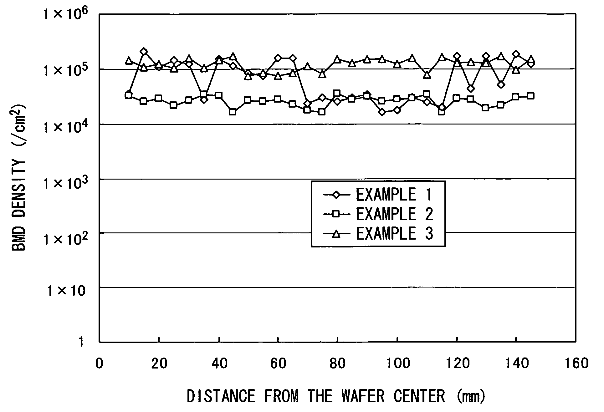
[0103] Using a growth apparatus having the undermentioned hot zone structure 1, under operation conditions determined by the above-described method, defect-free crystals of silicon single crystals having oxygen concentrations shown in Table 1 were grown as an embodiment of the present invention. A crucible is charged with 300 kg of polycrystalline silicon of high purity. A mixed gas mixing hydrogen into argon was used as an atmospheric gas. In the mixed gas, hydrogen gas was mixed to have a hydrogen molecule partial pressure of 240 Pa. The silicon single crystals were grown to have a diameter of 300 mm and a body length of 1600 mm.

TABLE 1Oxygen ConcentrationOSF ConcentrationExample(×1017 atoms / cm3)(pieces / cm2)Crystal Region113-1414PV Region +PI Region213-140PI Region314-150PI Region

[Hot Zone Structure 1]

[0104] The CZ furnace shown in FIG. 8 was used. The water cooling unit 8 had a cooling capacity expressed in the form of its inside diameter of 600 mm and height of 200 mm. The wa...

examples 4 and 5

[0105] Using a crystal growth apparatus having the undermentioned hot zone structure 2 defect-free crystals of silicon single crystals having oxygen concentrations shown in Table 2 were grown as comparative examples of the present invention. As like as Example 1, crucible is charged with 300 kg of polycrystalline silicon of high purity. Argon was used as an atmospheric gas. The silicon single crystals were grown to have a diameter of 300 mm and a body length of 1600 mm.

TABLE 2OxygenOSFExampleConcentrationConcentration(Comparative)(×1017 atoms / cm3)(pieces / cm2)Crystal Region411.5-12.570OSF Region +PV Region +PI Region513-14>1000OSF Region +PV Region +PI Region

[Hot Zone Structure 2]

[0106] A CZ furnace having neither the water cooling unit 8 nor the heat shield 7 was used. A horizontal magnetic field was supplied as in the case of the hot zone structure 1. A hot zone structure was provided to realize an axial thermal gradient Gc of 2.8° C. / mm at the central portion of the crystal bet...


PUM

PropertyMeasurementUnit
melting pointaaaaaaaaaa
temperatureaaaaaaaaaa
partial pressureaaaaaaaaaa

Abstract

In a method for growing a silicon single crystal, a silicon single crystal is grown by the Czochralski method to have an oxygen concentration of 12×1017 to 18×1017 atoms / cm3 on ASTM-F121 1979. A mixed gas of an inert gas and a gaseous substance containing hydrogen atoms is used as an atmospheric gas for growing the single crystal. A temperature of the silicon single crystal is controlled during the growth of the crystal such that the ratio Gc / Ge of an axial thermal gradient Gc at the central portion of the crystal between its melting point and its temperature of 1350° C. to an axial thermal gradient Ge at the periphery of the crystal between its melting point and its temperature of 1350° C. is 1.1 to 1.4. The axial thermal gradient Gc at the central portion of the crystal is 3.0 to 3.5° C. / mm.

Description

BACKGROUND OF THE INVENTION [0001] 1. Field of the Invention [0002] The present invention relates to a method for manufacturing a silicon wafer which has an oxide precipitate density to allow a sufficient gettering capability, and a method for growing a silicon single crystal used as a raw material for the silicon wafer. Particularly, the invention relates to a method for growing a silicon single crystal to effectively manufacture a silicon single crystal having a body portion comprising an oxide precipitation promoting region (PV region) and / or oxide precipitation inhibiting region (PI region). Priority is claimed on Japanese Patent Application No. 2005-179997, filed Jun. 20, 2005, and U.S. Provisional Patent Application No. 60 / 693,977 filed Jun. 27, 2005, the content of which is incorporated herein by reference. [0003] 2. Description of Related Art [0004] As a method for manufacturing a silicon single crystal as a raw material for a silicon wafer, a method for growing a silicon si...

Claims


Application Information

Patent Timeline
Patent Type & Authority Applications(United States)
IPC IPC(8): C30B21/04C30B13/00C30B28/08
CPCC30B15/04C30B29/06C30B15/14
Inventor INAMI, SHUICHITAKASE, NOBUMITSUKOGURE, YASUHIROHAMADA, KENNAKAMURA, TSUYOSHI
Owner SUMCO CORP
Learn More