Plasma film-forming method and plasma film-forming apparatus
a film-forming method and plasma technology, applied in the field of plasma-assisted deposition, can solve the problems of reducing the deposition rate, reducing the throughput of the process to a level unsuitable for mass production processes, and high plasma electron temperature, and achieve excellent electric characteristics and suppress the effect of excessive decomposition of source gas
- Summary
- Abstract
- Description
- Claims
- Application Information
AI Technical Summary
Benefits of technology
Problems solved by technology
Method used
Image
Examples
experiment 1
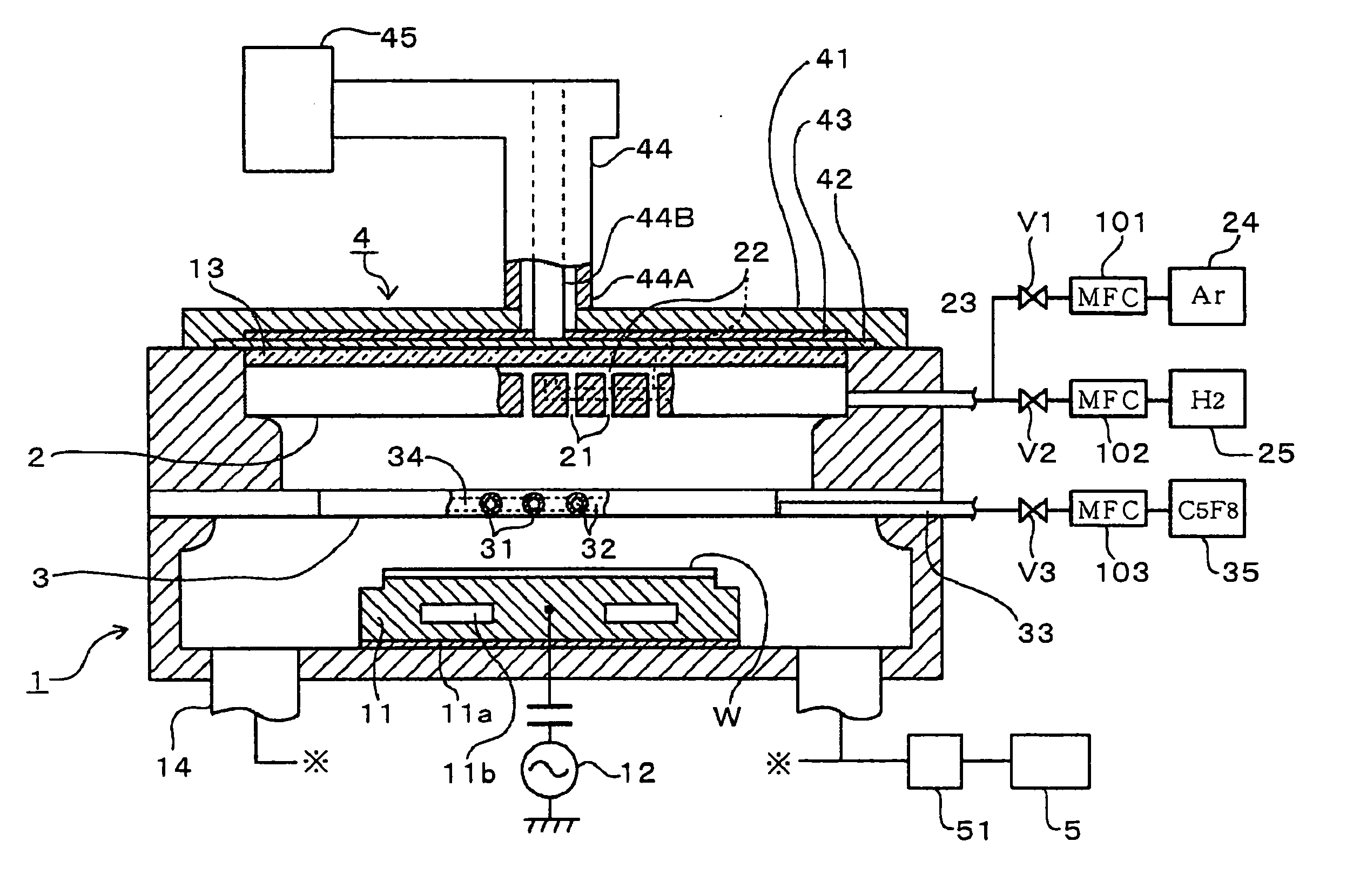
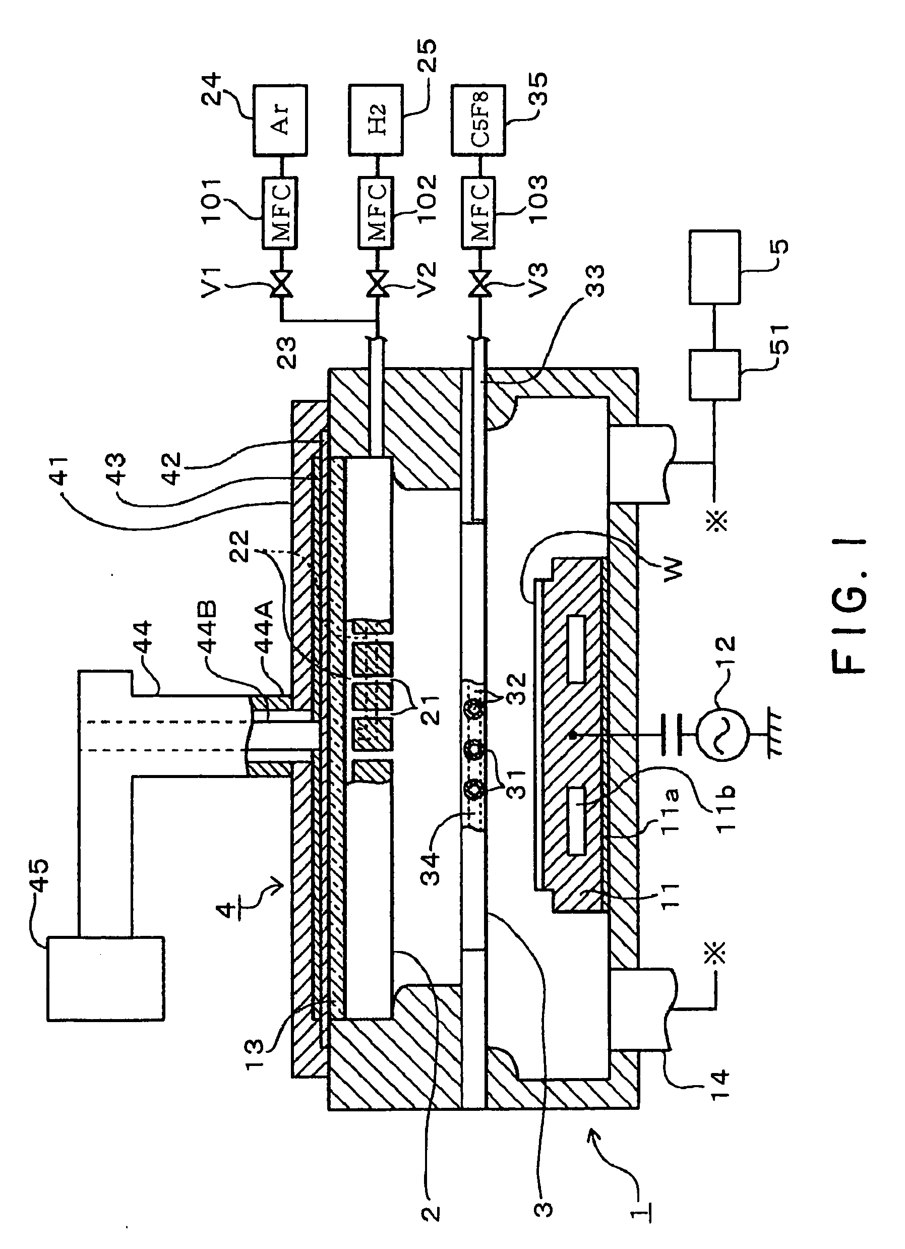
[0052] CF films were formed under various process conditions by the plasma-assisted deposition system shown in FIG. 1 and various source gases. The relative dielectric constants of the CF films and leakage currents flowed through the CF films were measured. FIG. 6 shows the measured results. In FIG. 6, leakage current is represented on the vertical axis and relative dielectric constant is represented on the horizontal axis. An electric field of 1 MV / cm was applied to the insulating film and leakage current flowed through the insulating film was measured. The inventors obtained a mass of data on source gases through experiments, only the typical data is shown in FIG. 6 because the data are analogous.
[0053] In FIG. 6, blank squares indicate data on the CF films formed by using C3F6 gas, blank triangles indicate data on the CF films formed by using C4F6 gas, solid squares indicate data on the CF films formed by using C4F8 gas and blank rhombuses indicate data on the CF films formed by...
experiment 2
[0060] CF films were formed under various process conditions by the plasma-assisted deposition system shown in FIG. 1 using C5F8 gas as a source gas for pressures of processing atmosphere (process pressures) of 6.65 Pa (50 mTorr), 13.3 Pa (100 mTorr), 19.95 Pa (150 mTorr) and 26.6 Pa (200 mTorr). The relative dielectric constants of the CF films and leakage currents flowed through the CF films were measured. FIG. 7 shows the measured results. In FIG. 7, leakage current is represented on the vertical axis and relative dielectric constant is represented on the horizontal axis. An electric field of 1 MV / cm was applied to the insulating film and leakage current flowed through the insulating film was measured. The process conditions are the distance between the second gas discharge head 3 and the wafer (FIG. 1), high-frequency power, the flow rate of Ar gas, the flow rate of the source gas and the temperature of the wafer. CF films were deposited by using various combinations of the proc...
PUM
| Property | Measurement | Unit |
|---|---|---|
| pressure | aaaaa | aaaaa |
| relative dielectric constant | aaaaa | aaaaa |
| magnetic field | aaaaa | aaaaa |
Abstract
Description
Claims
Application Information
 - R&D
- Intellectual Property
- Life Sciences
- Materials
- Tech Scout
- Unparalleled Data Quality
- Higher Quality Content
- 60% Fewer Hallucinations
Browse by: Latest US Patents, China's latest patents, Technical Efficacy Thesaurus, Application Domain, Technology Topic, Popular Technical Reports.
© 2025 PatSnap. All rights reserved.Legal|Privacy policy|Modern Slavery Act Transparency Statement|Sitemap|About US| Contact US: help@patsnap.com


