Method for manufacturing a semiconductor package with a laminated chip cavity
- Summary
- Abstract
- Description
- Claims
- Application Information
AI Technical Summary
Benefits of technology
Problems solved by technology
Method used
Image

Examples
first embodiment
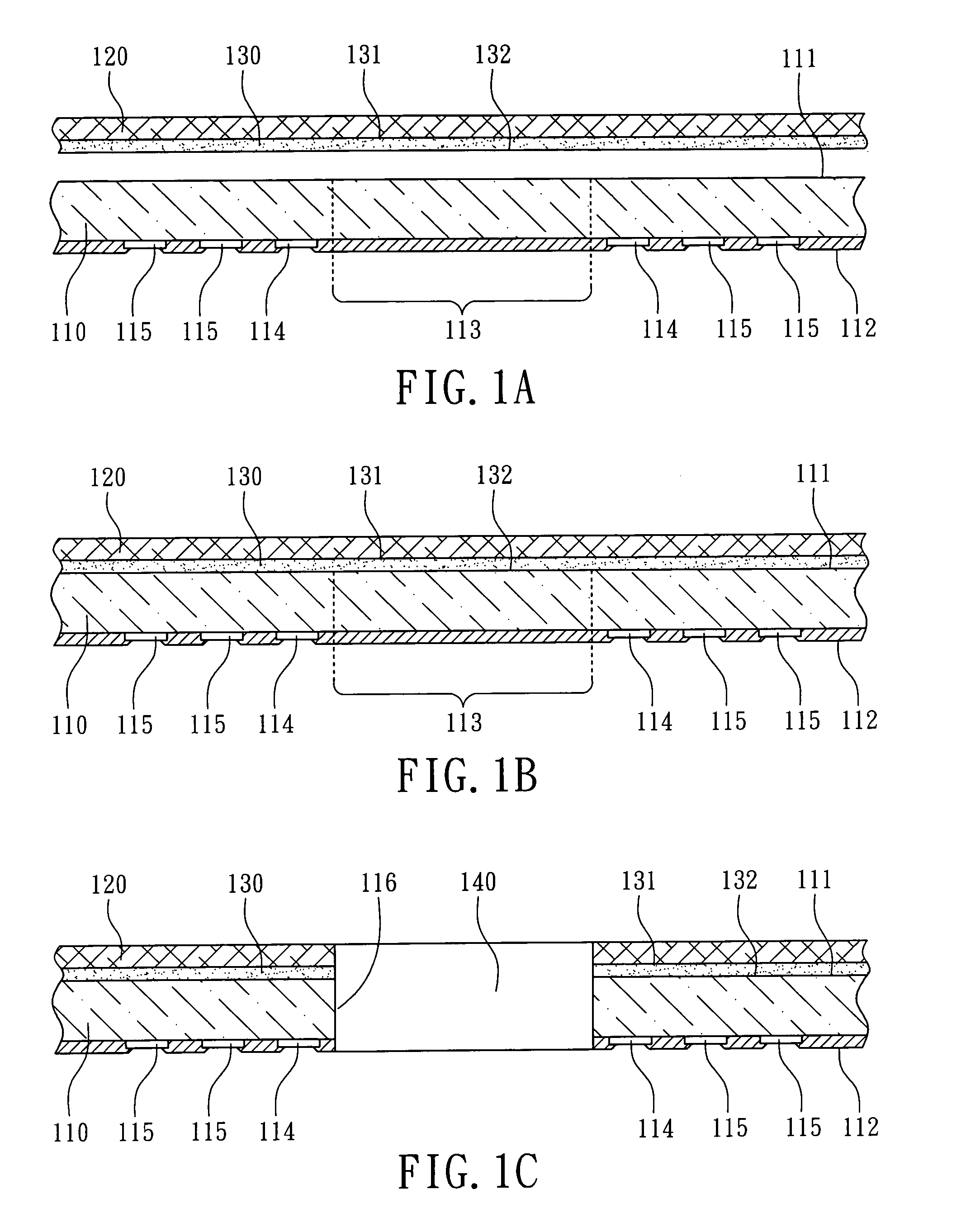
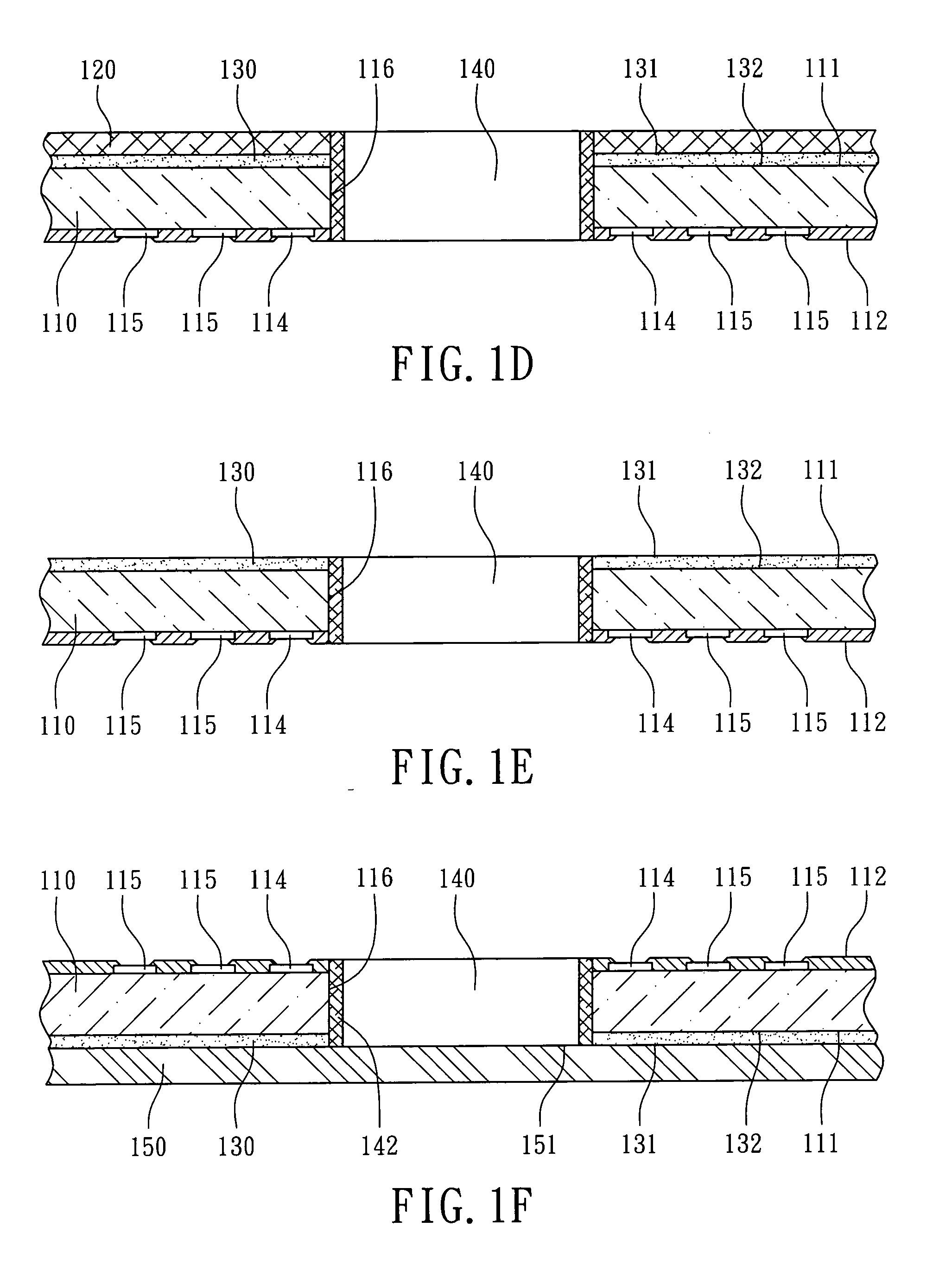
[0014] According to the present invention, a method for manufacturing a semiconductor package is illustrated in the As shown in FIG. 1A, initially a board 110 is provided, and a metal foil 120 with a layer of adhesive resin 130 is provided. The board 110 has a first surface 111 and a second surface 112 opposing to the first surface 111, and defines at least a region 113 for forming chip cavity inwall. In this embodiment, the board 110 is a substrate having circuit patterns and is suitable for forming a face-down chip cavity, such as a printed circuit board containing BT resin. The first surface 111 is utilized for attaching a carrier plate 150 (as shown in FIG. 1). A plurality of conductive fingers 114 for connecting with bonding wires and a plurality of ball pads 115 for connecting with solder balls are formed on the second surface 112. Generally, there is no need to coat any adhesive material on the first surface 111 of the board 110.
[0015] The metal foil 120 is preferably made o...
second embodiment
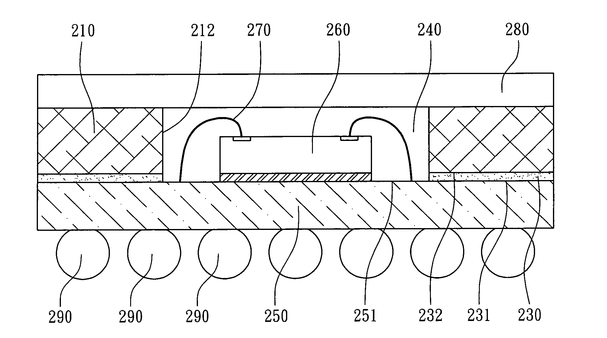
[0023] Moreover, the method for manufacturing a semiconductor package in accordance with the present invention can be applied for manufacturing semiconductor package of different packaging type, such as image sensor chip package with face-up chip cavity. the present invention is illustrated below. Referring to FIG. 4A, initially a board 210 is provided, which has a first surface 211 and a second surface 212 opposing to the first surface 211. In addition, a metal foil 220 with a layer of adhesive resin 230 is provided. In this embodiment, the board 210 is a substrate core made of prepreg including glass fiber. At least a region 213 for forming chip cavity inwall is defined in the board 210. The adhesive resin 230 is formed on one surface of the metal foil 220. The adhesive resin 230 has a first adhesive surface 231 attached to the metal foil 220 with a second adhesive surface 232 exposed.
[0024] Next, as shown in FIG. 4B, the metal foil 220 and the board 210 are laminated together, so...
PUM
 Abstract
Description
Claims
Application Information
 - R&D
- Intellectual Property
- Life Sciences
- Materials
- Tech Scout
- Unparalleled Data Quality
- Higher Quality Content
- 60% Fewer Hallucinations
Browse by: Latest US Patents, China's latest patents, Technical Efficacy Thesaurus, Application Domain, Technology Topic, Popular Technical Reports.
© 2025 PatSnap. All rights reserved.Legal|Privacy policy|Modern Slavery Act Transparency Statement|Sitemap|About US| Contact US: help@patsnap.com