Thin film transistor and method for production thereof
a technology transistors, applied in the direction of transistors, electroluminescent light sources, electric lighting sources, etc., can solve the problems of difficult to realize large-scale displays and varying properties of thin film transistors, and achieve uniform characteristic properties, increase driving current, and speed up
- Summary
- Abstract
- Description
- Claims
- Application Information
AI Technical Summary
Benefits of technology
Problems solved by technology
Method used
Image
Examples
first embodiment
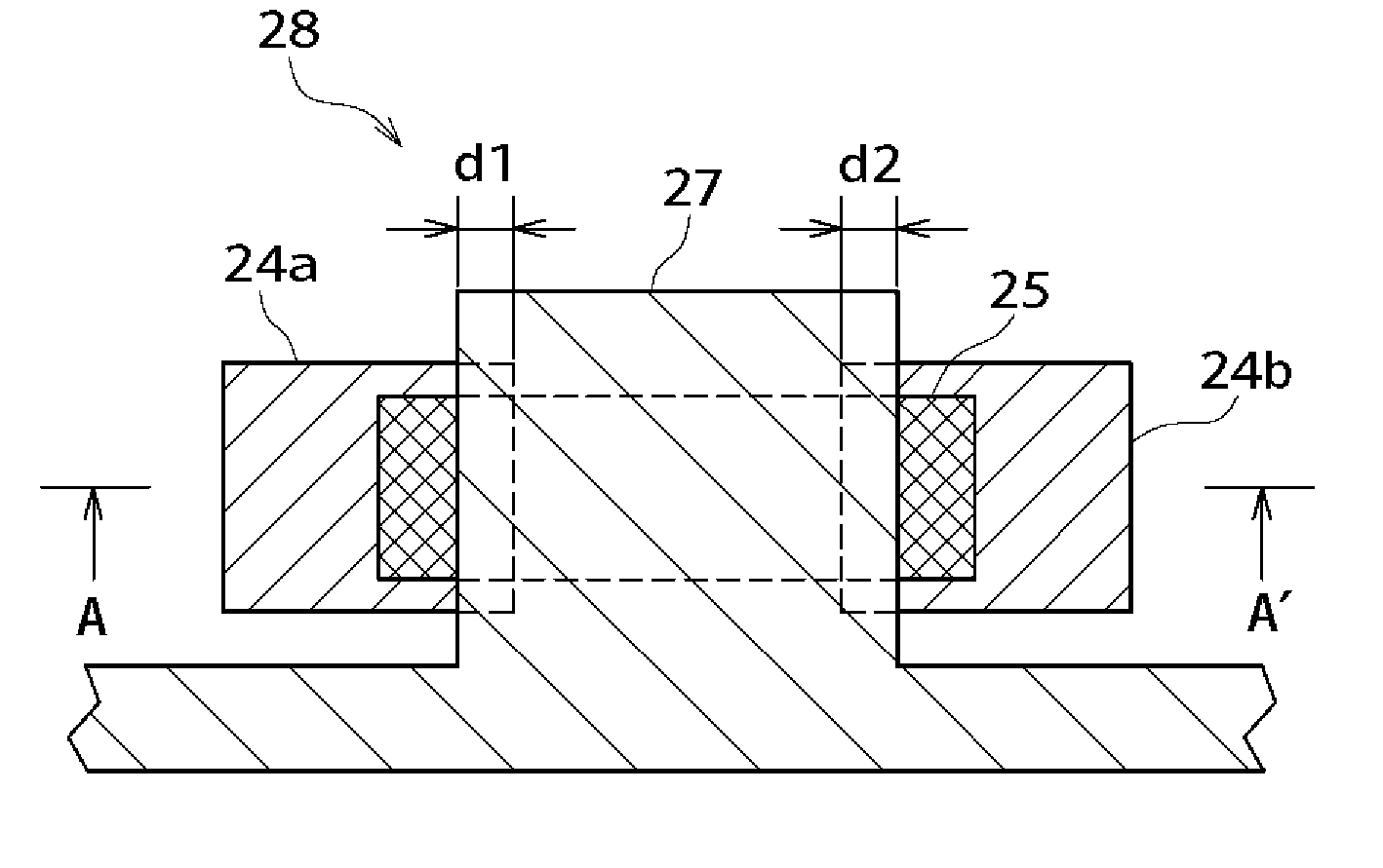
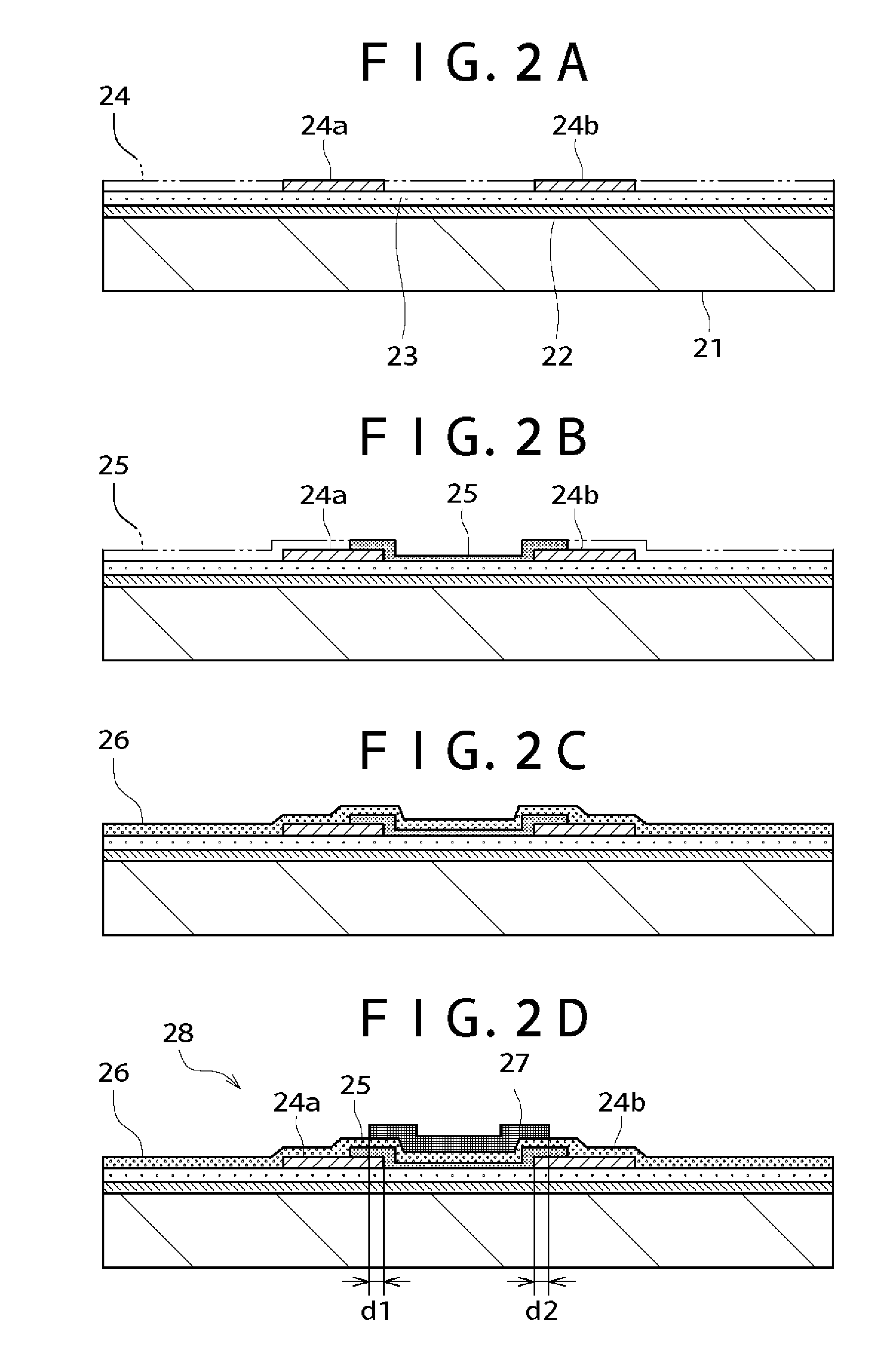
[0052]FIGS. 2A to 4B are sectional views which illustrate the method for producing thin film transistors in the first embodiment. The following is concerned with the method for producing a stacked TFT of top gate type as a thin film semiconductor device. The following is also concerned with the method for producing a display device with said stacked TFT's.
[0053] The first step is to prepare an insulating substrate 21 as shown in FIG. 2A. The substrate 21 may be AN635 or AN100 (from Asahi Glass) or Codel 1737 or Eagle 2000 (from Corning) or the like.
[0054] On the substrate 21 are sequentially formed a silicon nitride (SiNx) film 22 as a buffer layer and a silicon oxide film (SiOx) 23, which have a thickness ranging from about 50 to 400 nm.
[0055] Then, on the silicon oxide film 23 is formed by the reactive heat CVD process a source-drain layer 24 from polycrystalline silicon or polycrystalline silicon-germanium containing an n-type (or p-type) impurity. The source-drain layer 24 ma...
second embodiment
[0081] Sectional views of FIGS. 5 and 6 illustrate the method for producing thin film transistors in the second embodiment. The following is concerned with the method for producing a stacked TFT of bottom gate type as a thin film semiconductor device. The following is also concerned with the method for producing a display device with said stacked TFT's.
[0082] First, as shown in FIG. 5A, an insulating substrate 51 is coated with a conductive film of 50 to 250 nm thick of tantalum (Ta), molybdenum (Mo), tungsten (W), chromium (Cr), copper (Cu), or an alloy thereof, in the same way as in the first embodiment. Then, this conductive film is made into gate electrodes 52 by patterning.
[0083] Subsequently, as shown in FIG. 5B, a silicon nitride film 53a of 30 to 50 nm thick and a silicon oxide film 53b of 50 to 200 nm thick are sequentially formed by plasma CVD, atmospheric CVD, or reduced pressure CVD. The resulting laminate film is made into a gate insulating film 53.
[0084] Then, an ac...
PUM
 Abstract
Description
Claims
Application Information
 - R&D
- Intellectual Property
- Life Sciences
- Materials
- Tech Scout
- Unparalleled Data Quality
- Higher Quality Content
- 60% Fewer Hallucinations
Browse by: Latest US Patents, China's latest patents, Technical Efficacy Thesaurus, Application Domain, Technology Topic, Popular Technical Reports.
© 2025 PatSnap. All rights reserved.Legal|Privacy policy|Modern Slavery Act Transparency Statement|Sitemap|About US| Contact US: help@patsnap.com


