Thin film transistor substrate and process for producing the same
a technology substrates, applied in semiconductor devices, semiconductor/solid-state device details, instruments, etc., can solve the problems of uneven characteristic properties of thin film transistors, uneven length of side-etching and further length of ldd, and product yield decline, etc., to achieve uniform characteristic properties and high productivity
- Summary
- Abstract
- Description
- Claims
- Application Information
AI Technical Summary
Benefits of technology
Problems solved by technology
Method used
Image
Examples
example 1
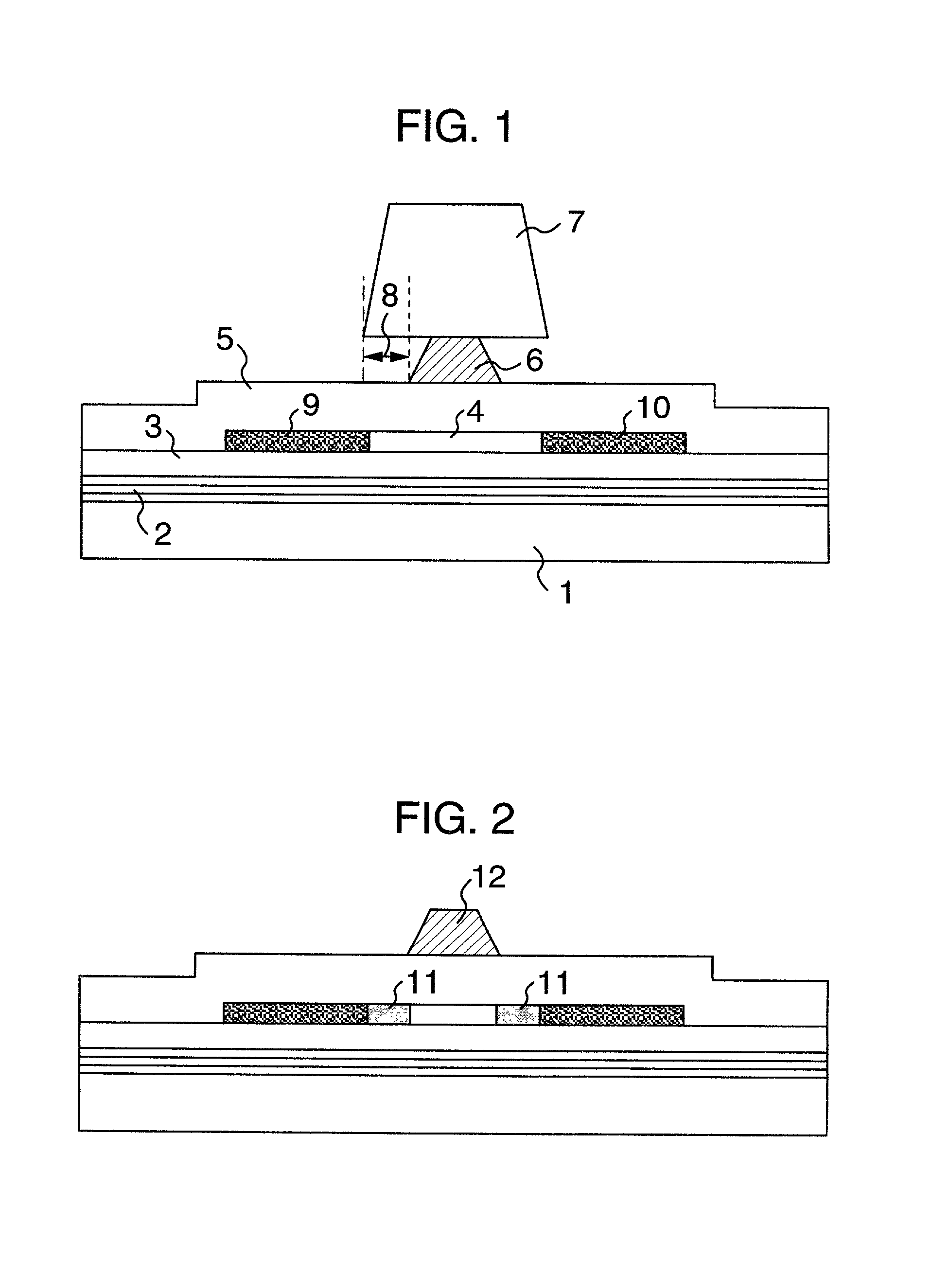
[0027] FIG. 1 and FIG. 2 illustrate the first example of the process for producing a thin film transistor substrate according to an embodiment of the present invention. Thus, a polycrystalline Si film 4 is formed on a glass substrate 1, which is a transparent insulator substrate, through intermediation of an undercoat (SiN) 2 and an undercoat (SiO.sub.2) 3 both provided for blocking the impurities released from the glass substrate. The polycrystalline Si film is formed by first forming an amorphous Si film by means of plasma CVD, followed by an annealing process by a dehydrogenating treatment at 400.degree. C. or below and crystallization by pulse excimer laser annealing.
[0028] After processing the polycrystalline Si film into an island-like form by photolithography, SiO.sub.2 film functioning as gate insulating film 5 is deposited by plasma CVD method using TEOS (tetraethoxysilane). Then, an electrically conductive film 6 made of Mo--W alloy is deposited up to a thickness of 150 nm...
example 2
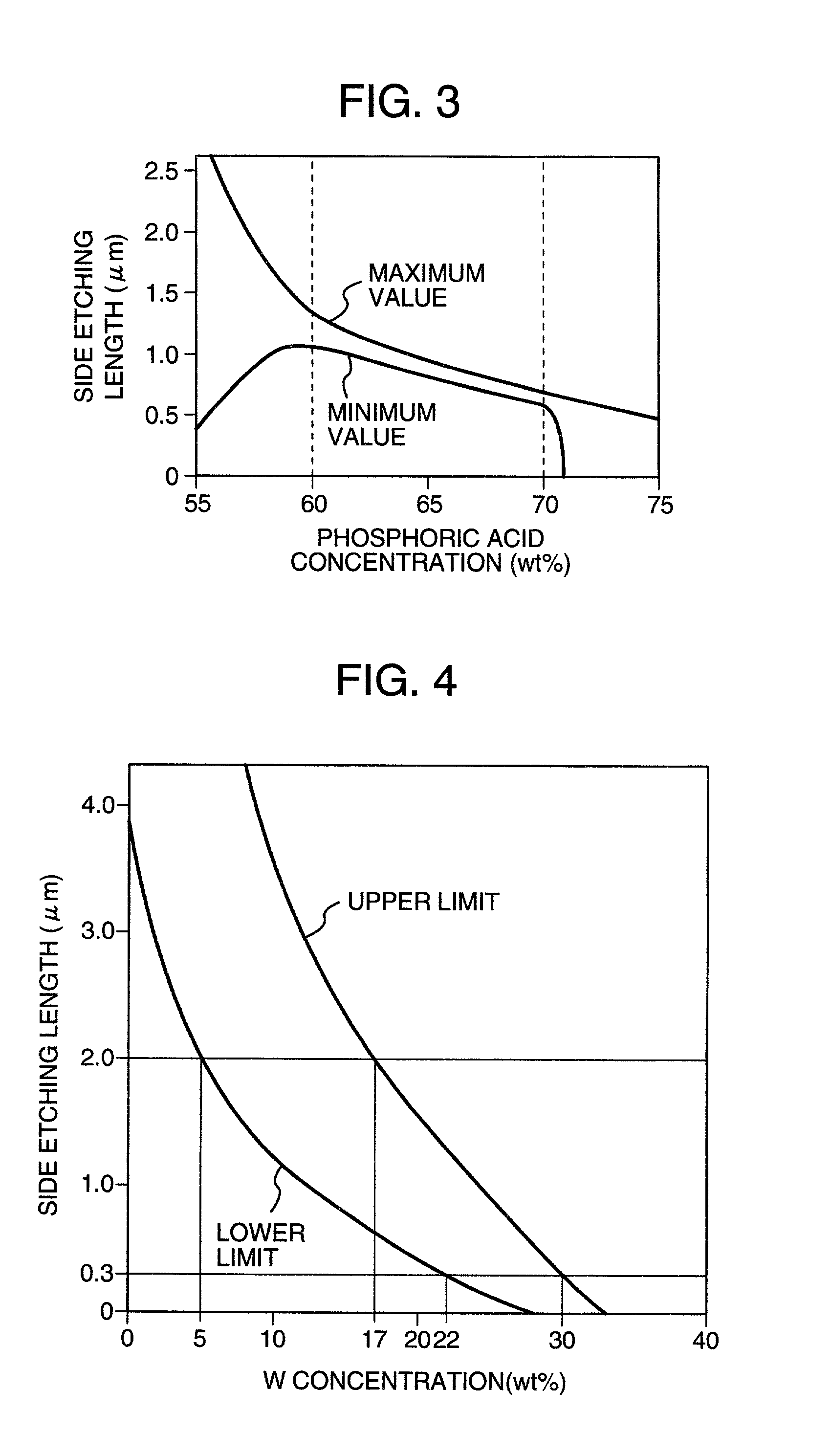
[0035] FIG. 5 illustrates an example of pixel in a liquid crystal display using a thin film transistor substrate according to the second example of the present invention, and FIG. 6 illustrates a section thereof at the line A-A'. A thin film transistor gate 12, a gate line 30 and a common electrode line 31 are formed from a Mo--W alloy containing 5% by weight (approximately 3 atomic %) of W. The thin film transistor gate 12, gate line 30 and common electrode line 31 are subjected to an etching treatment using an etching solution containing 70% by weight of phosphoric acid, and an LDD 11 having a length of 2 .mu.m is formed at the end of the gate 12 in a self-aligned manner.
[0036] On the gate, an interlayer insulating film 13 made of SiO.sub.2 is formed by Plasma CVD method using TEOS, and contact hole 14 is provided in the interlayer insulator film. A thin film transistor is connected to drain line 15 made of Ti / Al--Si alloy / Ti laminate film through the contact hole. Further, a tran...
example 3
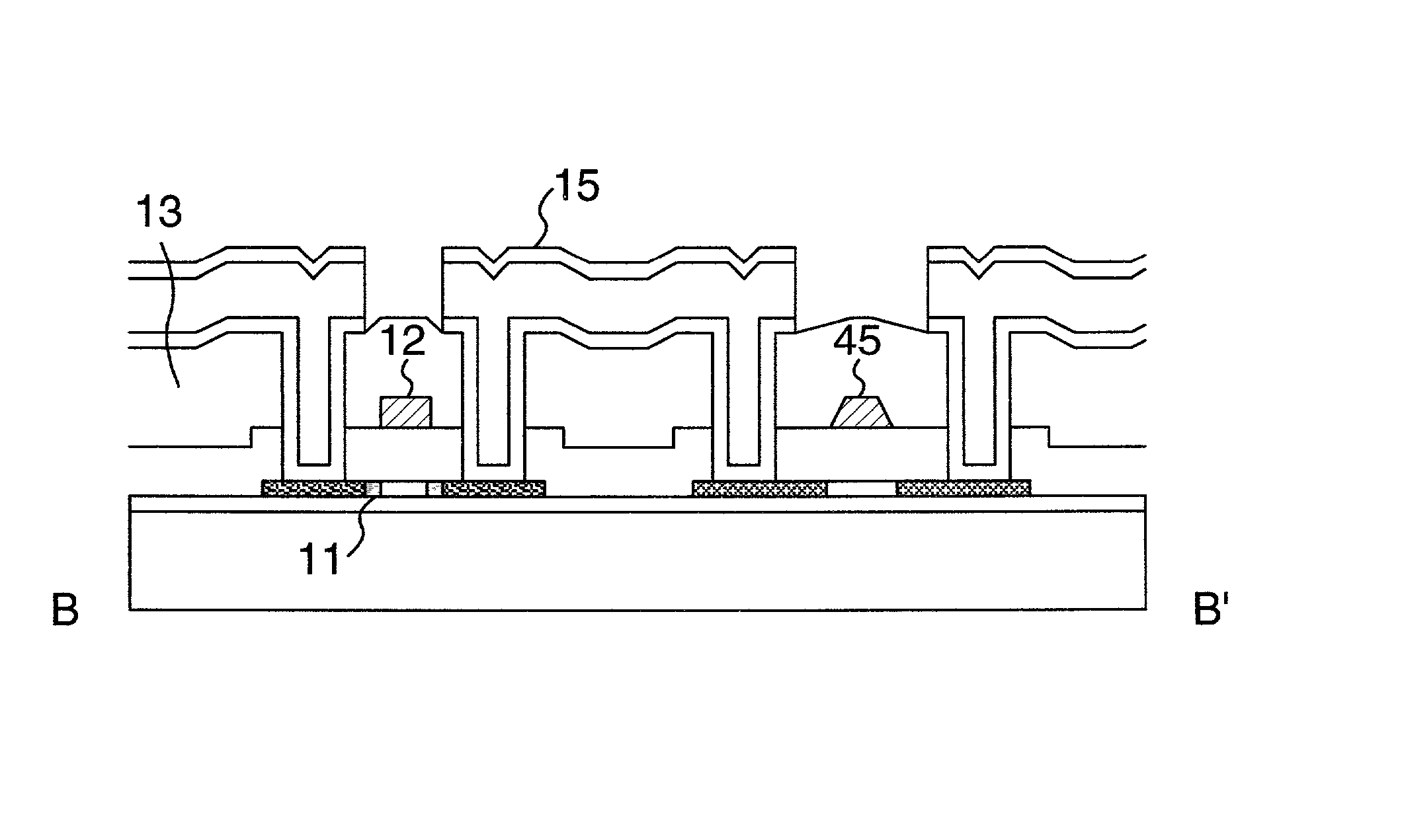
[0038] FIG. 7 illustrates the third example of the thin film transistor substrate according to the present invention, and FIG. 8 illustrates a sectional view thereof at the line B-B'. An N-type thin film transistor and a P-type thin film transistor are formed on a glass substrate 1 which is a transparent insulator substrate, and connected through drain line 15 made of Mo / Al--Si / Mo laminate film. The gates 12 and 45 of the thin film transistor are formed of a Mo--W alloy having a W concentration of 24% by weight (approximately 14 atomic %). On the terminal part of the gate 12 of the N-type thin film transistor, an LDD is formed in a self-aligned manner with the gate. In FIG. 7, 14 is contact hole; and in FIG. 8, 13 is an interlayer insulator film.
[0039] FIG. 9 through FIG. 13 illustrate an example of the process for producing the thin film transistor of FIG. 8. On a transparent insulator substrate 1, undercoat films 2 and 3, a polycrystalline Si film 4 and gate insulator film 5 are s...
PUM
| Property | Measurement | Unit |
|---|---|---|
| thickness | aaaaa | aaaaa |
| length | aaaaa | aaaaa |
| length | aaaaa | aaaaa |
Abstract
Description
Claims
Application Information
 - R&D
- Intellectual Property
- Life Sciences
- Materials
- Tech Scout
- Unparalleled Data Quality
- Higher Quality Content
- 60% Fewer Hallucinations
Browse by: Latest US Patents, China's latest patents, Technical Efficacy Thesaurus, Application Domain, Technology Topic, Popular Technical Reports.
© 2025 PatSnap. All rights reserved.Legal|Privacy policy|Modern Slavery Act Transparency Statement|Sitemap|About US| Contact US: help@patsnap.com


