
Method of performing physical vapor deposition with RF plasma source power applied to the target using a magnetron

a plasma source and magnetron technology, applied in the field of physical vapor deposition with rf plasma source power, can solve the problems of consuming production time, high production cost, adding cost, etc., and achieve the effect of low metal deposition ra

Active Publication Date: 2006-08-31
APPLIED MATERIALS INC
View PDF99 Cites 23 Cited by
  • Summary
  • Abstract
  • Description
  • Claims
  • Application Information

AI Technical Summary

Benefits of technology

The invention is about a method of physical vapor deposition that involves sputtering atoms from a metal target onto a workpiece. The method includes using a low level of target bias power to produce a low metal deposition rate on the workpiece. The method also includes ionizing the atoms sputtered from the metal target using a high level of VHF source power. The low level of target bias power can be as low as 500 Watts, and the method can use a solid large diameter RF feed rod that engages the metal sputter target. The workpiece can be electrostatically clamped to the workpiece support. The technical effect of this invention is to provide a method for physical vapor deposition that allows for precise control over the deposition rate and the ionization fraction of the atoms sputtered from the metal target.

Problems solved by technology

Because copper tends to diffuse over time through the insulator layer to cause catastrophic short circuiting, a barrier layer that blocks copper diffusion is placed between the copper material and the dielectric material wherever the two materials interface in the integrated circuit.
A problem arises in forming the vias extending vertically between the horizontal interconnect layers, as follows.
The interruption represented by the selective removal of the barrier layer entails a higher production cost and consumes production time.
While this dual-purpose reactor works extremely well, it does entail some additional expense.
In order to avoid process contamination, the re-sputtering coil is formed of pure tantalum, adding cost.
One problem is that the metal vapor deposition process can coat the ceiling with metal and thereby block inductive coupling from the coil antenna.
A more significant problem is that the RF plasma produced by the coil produces a high proportion of metal ions from the target, so that the wafer bias cannot be optimized for etch selectivity to horizontal surfaces without impacting (de-optimizing) the flux of metal ions / vapor from the target.
Typically, however, are large share of the copper ions are deposited on shields in the chamber and otherwise lost while traveling over this long distance.
In addition to the requirement for a copper PVD chamber and a barrier PVD chamber, a third chamber, an etch chamber, must be employed to carry out a pre-deposition cleaning process, since the copper PVD chamber and the barrier PVD / re-sputter chamber are not suitable for clean / etch processes.
Another problem is the tendency of the tantalum and / or tantalum nitride material deposited during formation of the barrier layer to deposit with non-uniform thickness along the via walls, and in particular to accumulate faster near the top corners of the vertical walls and thereby exhibit some tendency toward pinch-off.
Another problem that is to be solved is that, as technological advances dictate smaller geometries and higher aspect ratios for vias and other features, the degree of ionization of the sputtered material (e.g., copper) must be increased to achieve the requisite conformality of the deposited film.
Use of an electrostatic chuck limits the amount of VHF power that can be applied to the wafer.
The small gauge of the mesh (e.g., 100 microns) greatly limits the efficiency of the mesh as an RF radiator and limits the amount of RF power that can be applied to the mesh to as low as 1.5 kW maximum.

Method used


Image

  • Method of performing physical vapor deposition with RF plasma source power applied to the target using a magnetron
  • Method of performing physical vapor deposition with RF plasma source power applied to the target using a magnetron
  • Method of performing physical vapor deposition with RF plasma source power applied to the target using a magnetron

Examples


Embodiment Construction

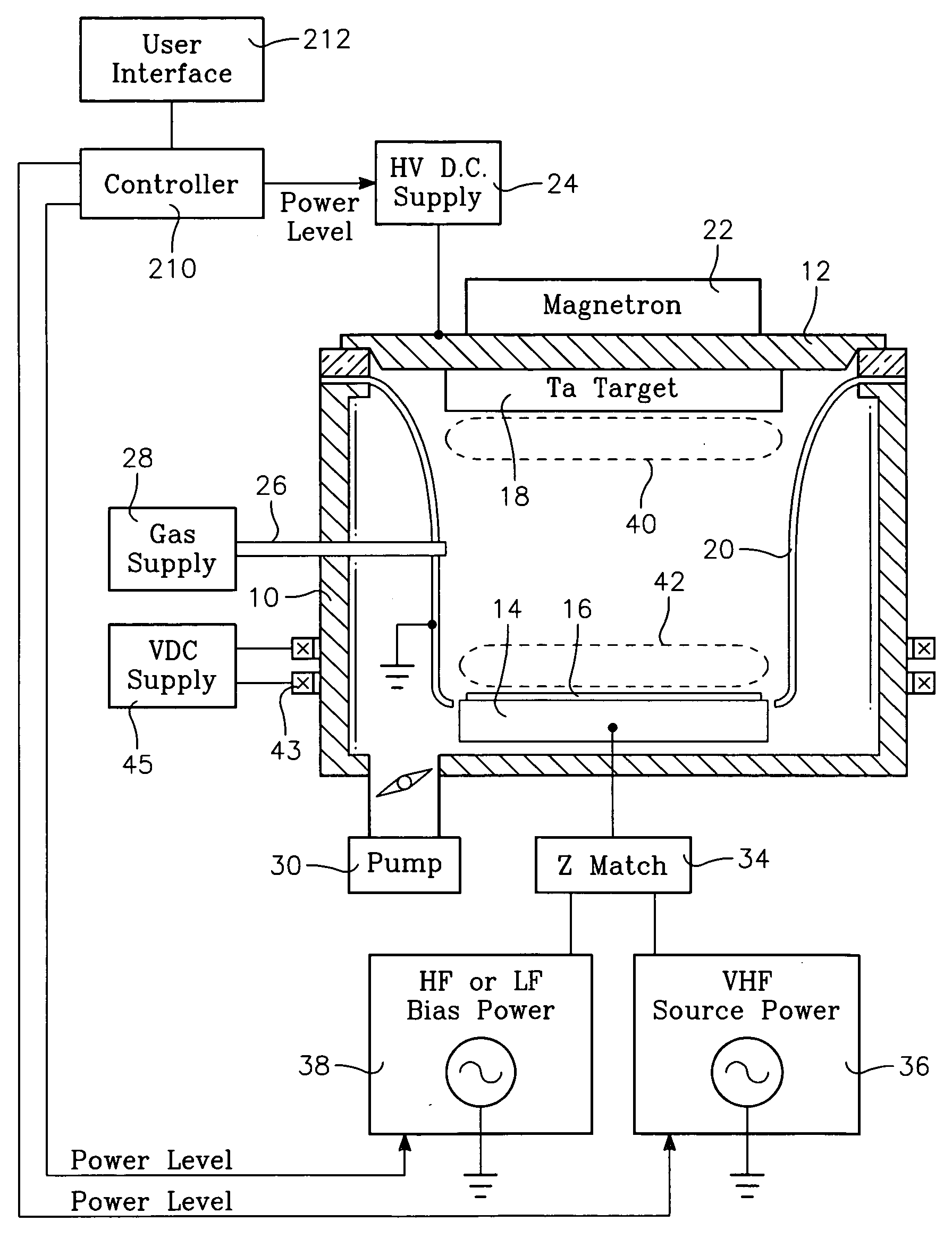
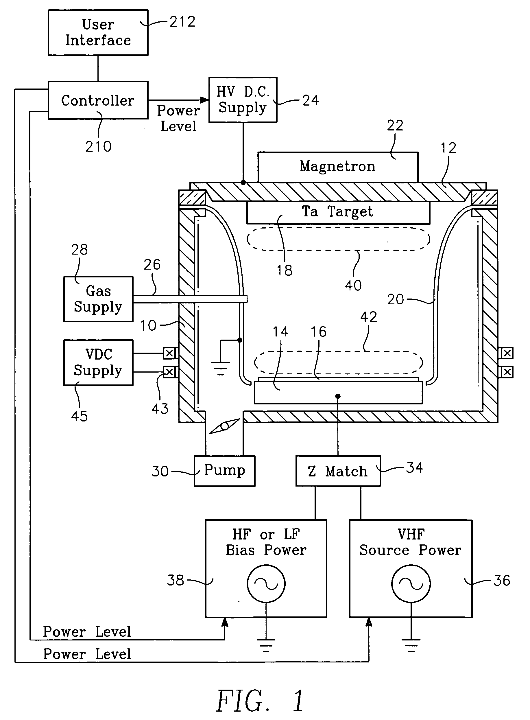
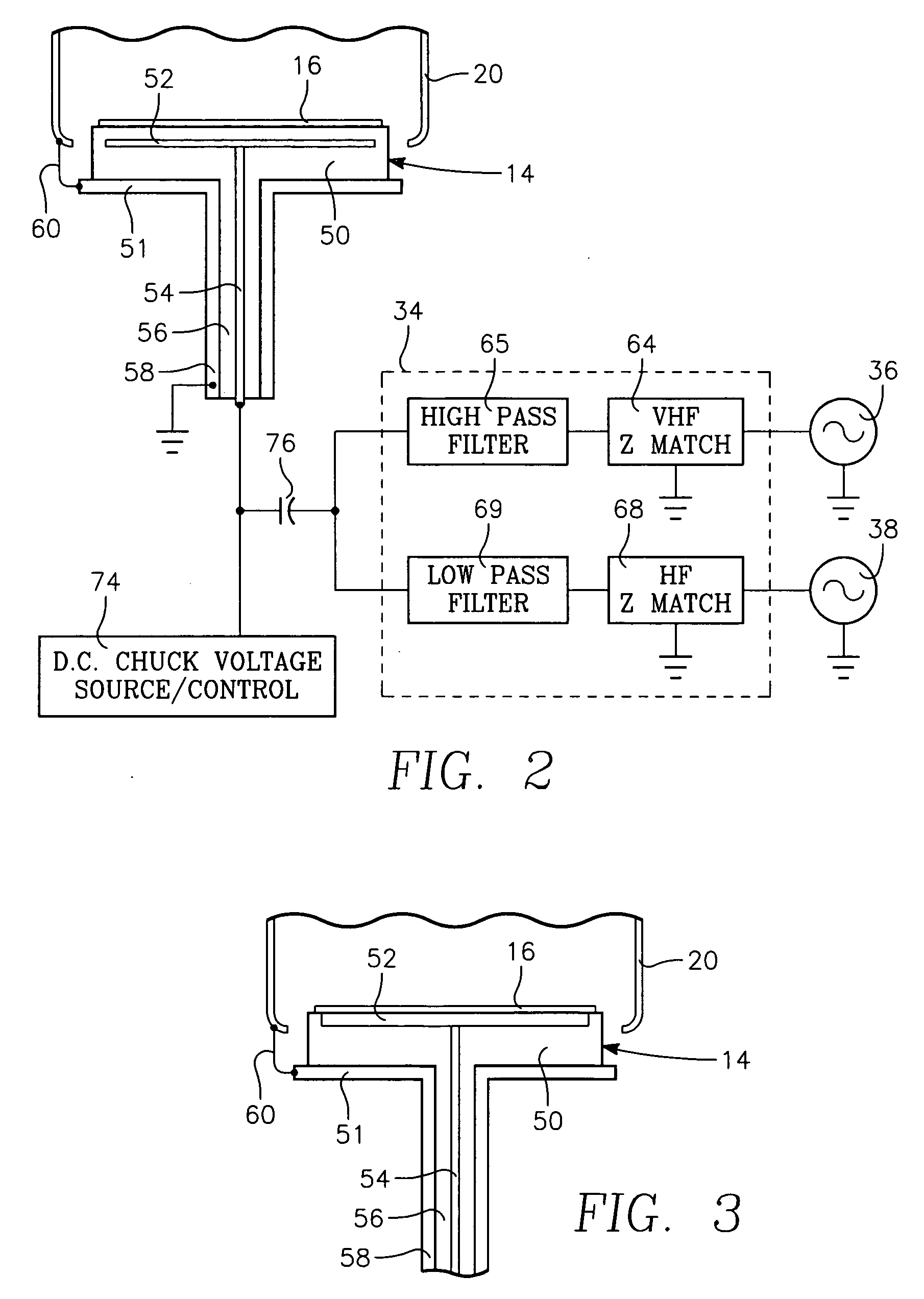
[0040] A plasma reactor forms barrier layers (such as a tantalum / tantalum nitride film or titanium / titanium nitride film) for conductors (such as copper, for which the barrier should be tantalum / tantalum nitride) in trenches or through vias between successive interconnection layers of an integrated circuit. The plasma reactor is capable of both physical vapor deposition and of highly selective re-sputtering to remove barrier material from the exposed horizontal surfaces of the underlying conductor constituting the floor of the via. Significantly, the reactor accomplishes all this without an internal coil that had previously been required for a fully and precisely controllable re-sputtering step. Instead, a plasma is formed near the wafer to perform the re-sputtering step. For this purpose a process gas such as argon may be introduced and source power is applied to the wafer at an RF frequency effective for capacitively coupling energy to kinetic electrons to excite argon plasma ions...


PUM

PropertyMeasurementUnit
poweraaaaaaaaaa
poweraaaaaaaaaa
sizesaaaaaaaaaa

Abstract

The invention concerns a method of performing physical vapor deposition in a reactor chamber on a workpiece positioned on a workpiece support facing the metal sputter target. The method includes sputtering atoms from the metal sputter target by applying a low level of target bias power to the metal sputter target to produce a correspondingly low metal deposition rate on the workpiece. The method further includes ionizing the atoms sputtered from the metal sputter target to an ionization fraction in excess of about 50% by applying a high level of VHF source power to the metal sputter target through a solid large diameter RF feed rod that engages the metal sputter target. The low level of target bias power can be as low as about 500 Watts although it may range up to about 2500 Watts. Preferably, the target bias power is D.C. power. The RF feed rod may be threadably engaged into a receptacle in the center of a top surface of the metal sputter target. Preferably, the method further includes electrostatically clamping the workpiece to the workpiece support.

Description

CROSS-REFERENCE TO RELATED APPLICATIONS [0001] This application is a continuation-in-part of U.S. application Ser. No. 11 / 052,011 filed Feb. 3, 2005, entitled “APPARATUS FOR METAL PLASMA VAPOR DEPOSITION AND RE-SPUTTER WITH SOURCE AND BIAS POWER FREQUENCIES APPLIED THROUGH THE WORKPIECE” by Karl M. Brown et al. and assigned to the present assignee.BACKGROUND OF THE INVENTION [0002] With recent technological advances in integrated circuit design, there are now as many as six to ten interconnect layers of a multilayer interconnect structure overlying the semiconductor transistors. Insulator layers separate the successive conductor layers. The conductor interconnect layers can have completely different conductor patterns and are connected to one another and to the transistor layer at different locations through vias extending vertically through the insulator layers. It is the formation of the vias with which the present invention is concerned. [0003] To reduce resistive power losses in...

Claims


Application Information

Patent Timeline
Patent Type & Authority Applications(United States)
IPC IPC(8): B23K15/00
CPCC23C14/046C23C14/345C23C14/358H01J37/32082H01L21/76844H01J37/3408H01L21/2855H01L21/76843H01J37/32706
Inventor BROWN, KARL M.PIPITONE, JOHNMEHTA, VINEET
Owner APPLIED MATERIALS INC
Learn More