Electrostatic discharge circuit

Inactive Publication Date: 2006-08-24
SAMSUNG ELECTRONICS CO LTD
View PDF8 Cites 15 Cited by
  • Summary
  • Abstract
  • Description
  • Claims
  • Application Information

AI Technical Summary

Benefits of technology

[0009] Example embodiments of the present invention are directed to an electrostatic discharge circuit, with a lower trigger voltage and / or a faster reaction time.

Problems solved by technology

A well-known cause of failure in electronic integrated circuits is exposure to large and / or sudden electrostatic discharge (ESD).
The discharge can cause damage to the integrated circuit as a result of dielectric breakdown of oxides and / or other thin films, and also by higher levels of conduction through relatively small areas of the integrated circuit arising from reverse breakdown of p-n junctions on the circuit.
In particular, as a result of higher current density and lower voltage tolerance, as ICs become smaller and / or faster, the susceptibility of their protection circuits to damage may increase.
Still further, silicided source / drain diffusion areas may also lead to current localization by concentrating current flow at the surface of devices, as well as, reducing the ballasting resistance needed to distribute the current.
Additionally, thinner gate oxides of MOS transistors may be more susceptible to high-field stress, for example, dielectric breakdown.
In particular, if the first breakdown voltage or trigger voltage is higher than the breakdown voltage of the gate dielectric of a MOS transistor, the ESD protection scheme may fail to protect the internal circuit and the internal circuit may be destroyed.
Further, if a response time of the ESD triggering is delayed, the ESD protection scheme may fail to protect a high speed or higher frequency integrated circuit, due to an initial build-up of high voltage or large current.

Method used


Image

  • Electrostatic discharge circuit
  • Electrostatic discharge circuit
  • Electrostatic discharge circuit

Examples


Embodiment Construction

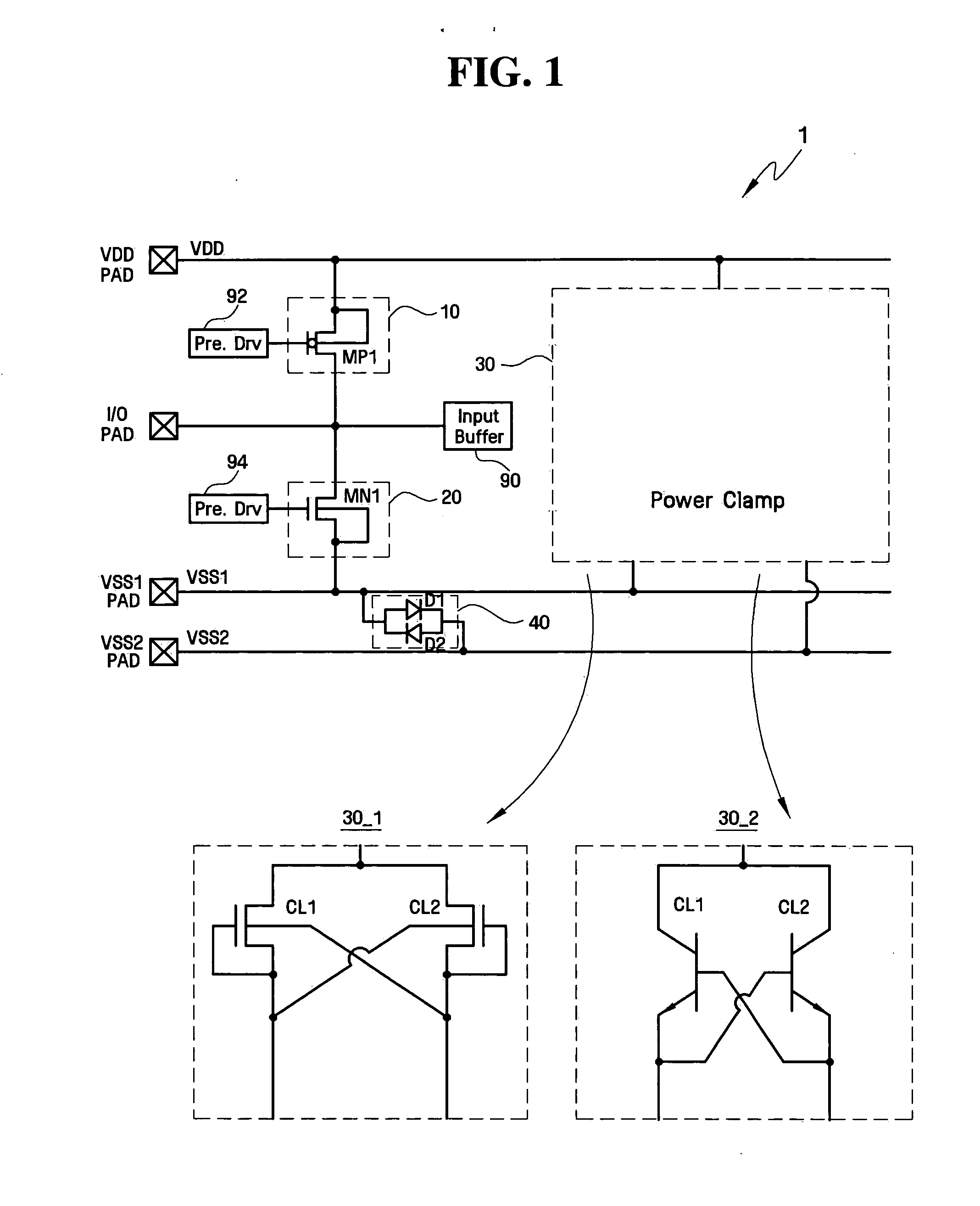
[0073]FIG. 1 illustrates an electrostatic discharge circuit in accordance with an example embodiment of the present invention. As shown in FIG. 1, the example electrostatic discharge circuit 1 may include a pull-up device 10, a pull-down device 20, a power clamp 30, and / or a transfer circuit 40. The electrostatic discharge device 1 may be connected to a supply voltage, for example, a VDD pad or VDD terminal, which may supply a positive supply voltage, for example, a VDD signal, an I / O pad or I / O terminal, which may supply an I / O signal, and at least one ground or reference supply voltage, for example, a VSS pad or VSS terminal, for example, VSS1 pad and VSS2 pad, which may supply VSS1 and VSS2 signals, respectively.

[0074] In another example embodiment, the electrostatic discharge device 1 may further include a pre-driver 92 connected to the pull-up device 10 and / or a pre-driver 94 connected to the pull-down device 20, and / or an input buffer 90. As shown in FIG. 1, the I / O pad may b...


PUM


Abstract

An electrostatic discharge circuit, connected between at least three terminals, the electrostatic discharge circuit including at least one electrostatic discharge circuit element further including at least one circuit element including a body in a floating state. The body in a floating state may provide a path to discharge an electrostatic current. The electrostatic discharge circuit may be a pull-up circuit, a plurality of pull-up circuits, a pull-down circuit, a plurality of pull-down circuits, a power clamp, a plurality of power clamps, or other similar circuit or circuits. The at least three terminals may include one or more power terminals, one or more ground terminals, and / or one or more I / O terminals.

Description

PRIORITY STATEMENT [0001] This U.S. non-provisional application claims priority under 35 U.S.C. § 119 to Korean Patent Application No. 2005-0015543, filed on Feb. 24, 2005, the entire contents of which are incorporated by reference. BACKGROUND OF THE INVENTION [0002] A well-known cause of failure in electronic integrated circuits is exposure to large and / or sudden electrostatic discharge (ESD). A built-up electrostatic charge may be quickly discharged when the charged device comes into contact with an integrated circuit, for example, when portions of the circuit are connected to power supplies, including ground. The discharge can cause damage to the integrated circuit as a result of dielectric breakdown of oxides and / or other thin films, and also by higher levels of conduction through relatively small areas of the integrated circuit arising from reverse breakdown of p-n junctions on the circuit. [0003] Electrostatic discharge (ESD) may have an effect on the reliability of integrated...

Claims


Application Information

Patent Timeline
IPC IPC(8): H01R13/64
CPCH01L27/0266H04B3/54
Inventor JEON, CHAN-HEE
Owner SAMSUNG ELECTRONICS CO LTD
Why Eureka
Try Eureka