Wiring board and capacitor to be built into wiring board

a wiring board and capacitor technology, applied in the direction of fixed capacitors, cross-talk/noise/interference reduction, fixed capacitor details, etc., can solve the problems of thermal stress, small and complicated wiring, and the pattern of the connecting via, so as to reduce the number of connecting steps, reduce the height of the entire board, and eliminate thermal stress disconnections or the like.

Active Publication Date: 2006-08-10
NGK SPARK PLUG CO LTD
View PDF8 Cites 30 Cited by
  • Summary
  • Abstract
  • Description
  • Claims
  • Application Information

AI Technical Summary

Benefits of technology

[0008] It is an object of the present invention to provide a wiring board wherein disconnections or the like due to thermal stress are substantially eliminated, the height of the entire board connecting structure is reduced and the number of connecting steps needed is also reduced.

Problems solved by technology

However, the gaps between terminals differ greatly for the terminal array of the integrated circuit as compared with the terminal array on the mother board.
When the terminal gap on the IC side is greatly different from the terminal gap on the side of the main board (mother board) to which the IC side is to be connected, the wiring needed for conversion, and the pattern of the connecting vias, tend to be quite small and complicated as the number of terminals involved increases.
This difference can potentially cause a defect such as peeling of the solder.
However, with ceramic package boards, because the wiring portion is formed by using printing and calcining of a metal paste, it is more difficult to miniaturize the wiring portion, and to thus provide a highly integrated wiring board, than with organic package boards which, as noted above, can be made using lithography techniques.
Thus, the amount of reduction in the terminal gaps on the side of the semiconductor integrated circuit element is limited.
However, with this structure, it is difficult to comply with the very small size requirement because the dimension of the board connecting structure in the heightwise direction is increased by the increase in the number of the intermediate boards.
For this reason, the multistage board connecting structure is not an attractive candidate for this application.

Method used


Image

  • Wiring board and capacitor to be built into wiring board
  • Wiring board and capacitor to be built into wiring board
  • Wiring board and capacitor to be built into wiring board

Examples


Embodiment Construction

[0068] Preferred embodiments of the present invention are described below with reference to the drawings.

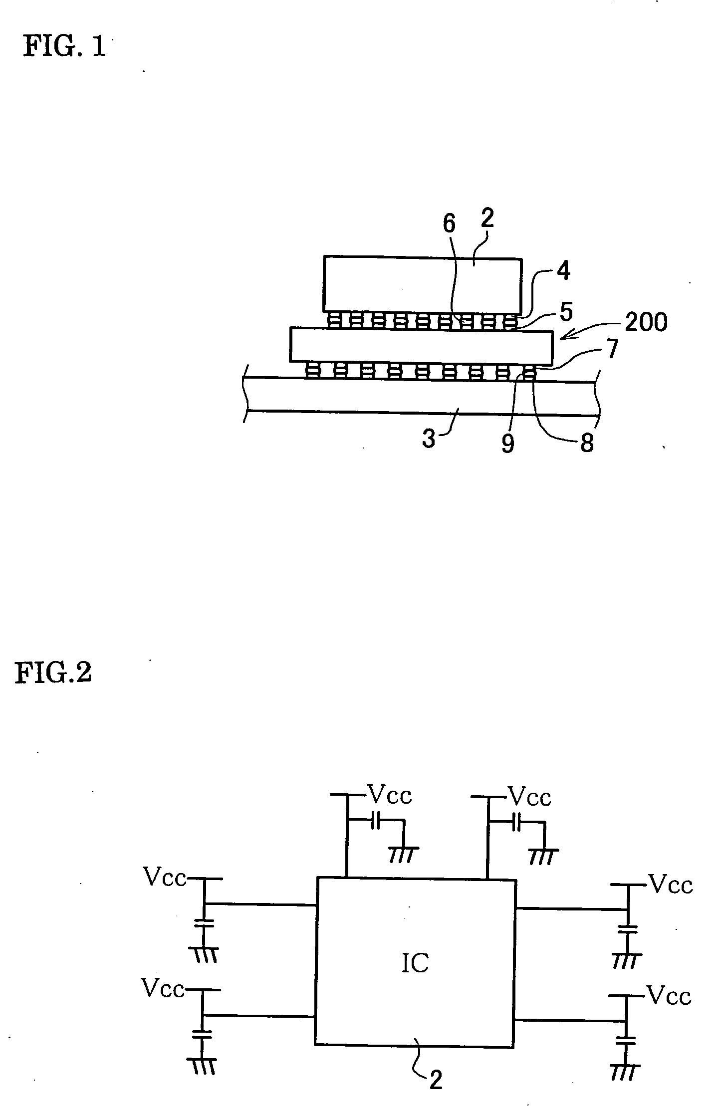
[0069]FIG. 1 illustrates wiring board construction wherein an intermediate board (wiring board) 200 according to a first embodiment of a wiring board of the present invention is arranged between a semiconductor integrated circuit element 2 and a main board 3. Further, with respect to the terminology used hereinbelow the first main surfaces of the planar or plate-like members of this embodiment are the surfaces that face upwardly in the drawing, and the second main surfaces are the surfaces which face downwardly.

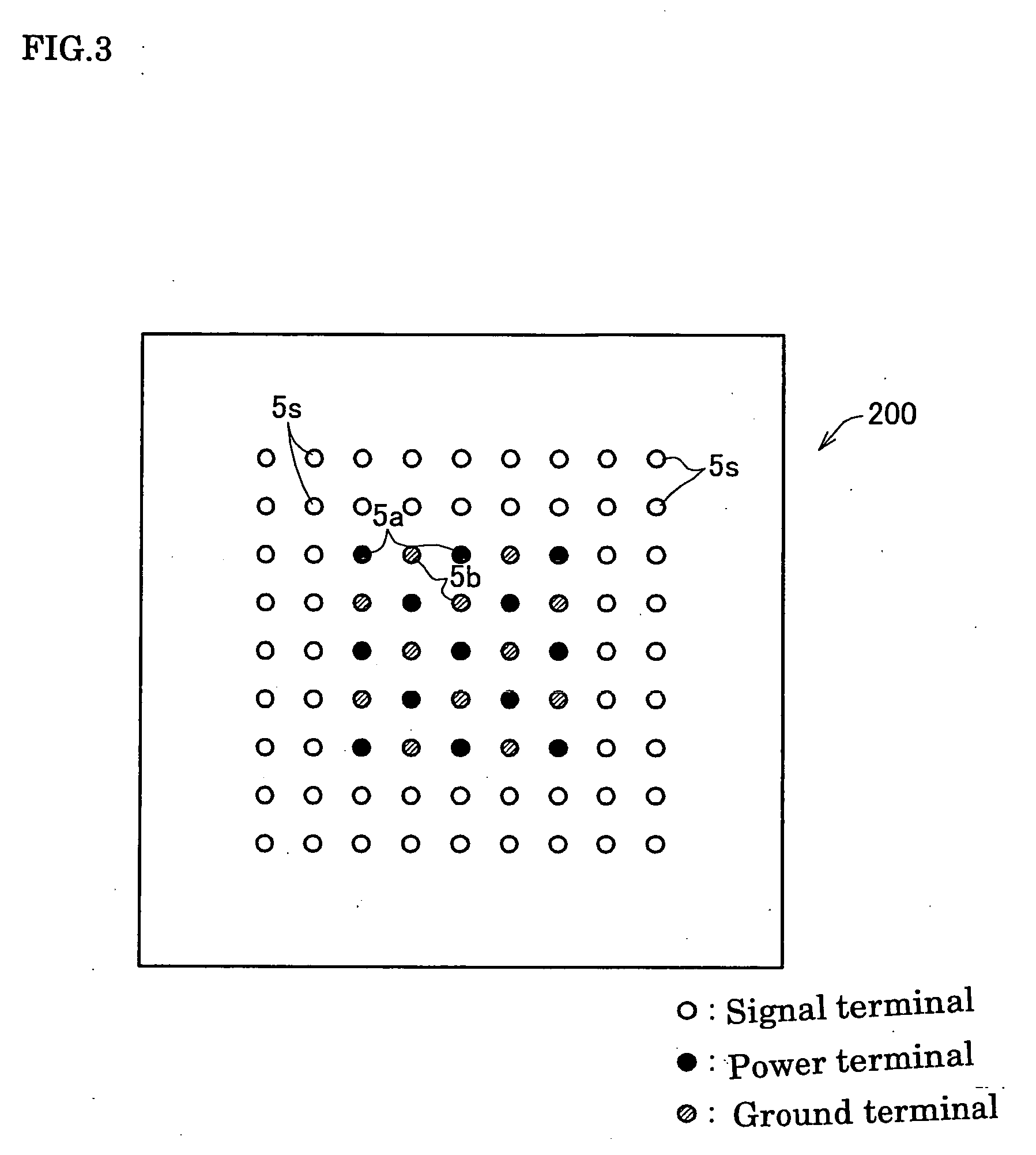
[0070] As shown in FIG. 1, the semiconductor integrated circuit element 2 includes a side terminal array 4 which is comprised of a plurality of signal terminals, a power source terminal and a ground terminal on the second main surface. The terminals of the side terminal array 4 is flip-chip connected to the terminals of a first terminal array 5 formed on the first main s...


PUM


Abstract

An intermediate board has a board core formed by a main core body and a sub-core portion. The main core body has a plate-like shape and includes an open sub-core housing portion in which the sub-core portion is housed. A first terminal array of the board core has an area that overlaps an orthogonal projection of the sub-core portion. The latter incorporates a laminated ceramic capacitor formed by first and second conductor layers with a ceramic (dielectric) layer therebetween. The first layer is connected to first and second side terminals of a first type while the second layer is connected to first and second side terminals of a second type. The housing portion has an inner edge which, in cross section, is of a quadrate shape, and a radius portion is formed at each corner having a dimension of between 0.1 and 2 mm.

Description

TECHNICAL FIELD [0001] The present invention relates to a wiring board and to a capacitor to be built into the wiring board. RELATED BACKGROUND ART [0002] In recent years, semiconductor integrated circuit elements such as CPUs, and other LSIs which operate at high speeds, have been made increasingly smaller in size, and thus the number of signal terminals, power source terminals and / or ground terminals has increased, and the distance between terminals has been reduced. A popular technique involves the provision of a terminal array comprising an integrated circuit wherein a large number of terminals are connected to a mother board using so-called flip-chip connections. However, the gaps between terminals differ greatly for the terminal array of the integrated circuit as compared with the terminal array on the mother board. Because of this, an intermediate wiring board is required in eliminating this difference in the terminal spacing. [0003] So-called organic package boards in such i...

Claims


Application Information

Patent Timeline
IPC IPC(8): H05K1/16
CPCH01G2/06H01L2224/16235H01L23/49838H01L23/50H01L24/10H01L2224/16225H01L2924/0102H01L2924/01078H01L2924/01079H01L2924/09701H01L2924/14H01L2924/1423H01L2924/15174H01L2924/15311H01L2924/3011H05K1/0231H05K1/185H05K3/4602H05K2201/10674H05K2201/10712H01L2924/01012H01L23/49822H01L2224/0554H01L2224/05568H01L2224/05573H01L2924/00014H01L2924/12042H01L2924/00H01L2224/05599H01L2224/0555H01L2224/0556H01L23/12H05K1/14
Inventor MURAMATSU, MASAKIYURI, SHINJIURASHIMA, KAZUHIROYAMAMOTO, HIROSHISEKI, TOSHITAKESATO, MOTOHIKO
Owner NGK SPARK PLUG CO LTD
Why Eureka
Try Eureka