
Integrated packaged having magnetic components

Active Publication Date: 2006-07-13
LITTELFUSE INC
View PDF6 Cites 68 Cited by
  • Summary
  • Abstract
  • Description
  • Claims
  • Application Information

AI Technical Summary

Benefits of technology

[0010] In the case of pre-assembled substrates, the assembly can occur in a snapstrate, which can be singulated after component assembly, wire bonding, and other substrate operations. The 8L-PDIP Snapstrate is an example of this technique, which provides lower assembly costs.
[0011] Yet another embodiment relates to a BGA package with a groove and holes for magnetic components. For example, a grooved PCB panel, which is milled or routed prior to singulation into substrate array, is provided. This makes the grooves more economical, and controllable. The groove is configured to receive the I-bar and bonded thereto, thereby providing a flat package bottom that is suitable for standard BGA package assembly. The groove may be configured to receive other magnetic components in other applications. For example, the groove may be implemented to receive a plate in an application for DC-DC converters.
[0013] The BGA provides a lower profile package and smaller footprint size. In the case of isolated input / output products, a first set of balls associated with an input die and a second set of balls associated with an output die are placed on the opposite ends of the package to provide a large creepage path for the required voltage isolation. Each of the first and second set of balls may include one or more rows of balls according to application. In the case of DC-DC Converter, and other isolated products that dissipate significant power, the BGA configuration provides excellent power dissipation or low thermal resistance, while maintaining a large creepage distance for voltage isolation.
[0014] In yet another embodiment, a packaged device includes a substrate having first and second dielectric layers, the first dielectric layer having a first winding defined thereon, the second dielectric layer having a second winding defined thereon. A magnetic assembly is formed on the substrate. An input die provided on the first dielectric layer is configured to receive a first signal and transmit a second signal to the magnetic assembly. An output die provided on the first dielectric layer is configured to receive the second signal via the magnetic assembly and output a third signal to an external node. A package material is provided over the magnetic assembly, the input die, and the output die to protect the magnetic assembly, the input die, and the output die from physical and environmental damage.
[0015] The magnetic assembly is a transformer and facilitates in isolating the input and output functions, so that the components (e.g., the die, wiring, and pins) on the input side are isolated from those on the output side. The magnetic assembly includes a U-core and an I-bar. The substrate includes a third dielectric layer having a groove to receive the I-bar, wherein the third dielectric layer is a lower dielectric layer and the first dielectric layer is an upper dielectric layer.

Problems solved by technology

However, the required voltage isolation capacity tends to be very large in certain applications, e.g., 3750 volts or more, to protect against sudden spikes or fault conditions.
Such a transformer requires one or more magnetic components and windings that are generally bulky.
Accordingly, the transformer is placed external to the packaged gate driver, which requires a large footprint and increased manufacturing cost.
Such a device, which uses optical coupling, does not provide as good a performance as one based on magnetic coupling.

Method used


Image

  • Integrated packaged having magnetic components
  • Integrated packaged having magnetic components
  • Integrated packaged having magnetic components

Examples


Embodiment Construction

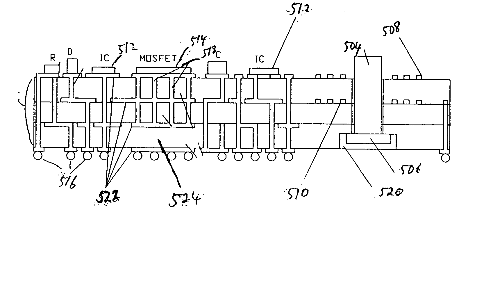
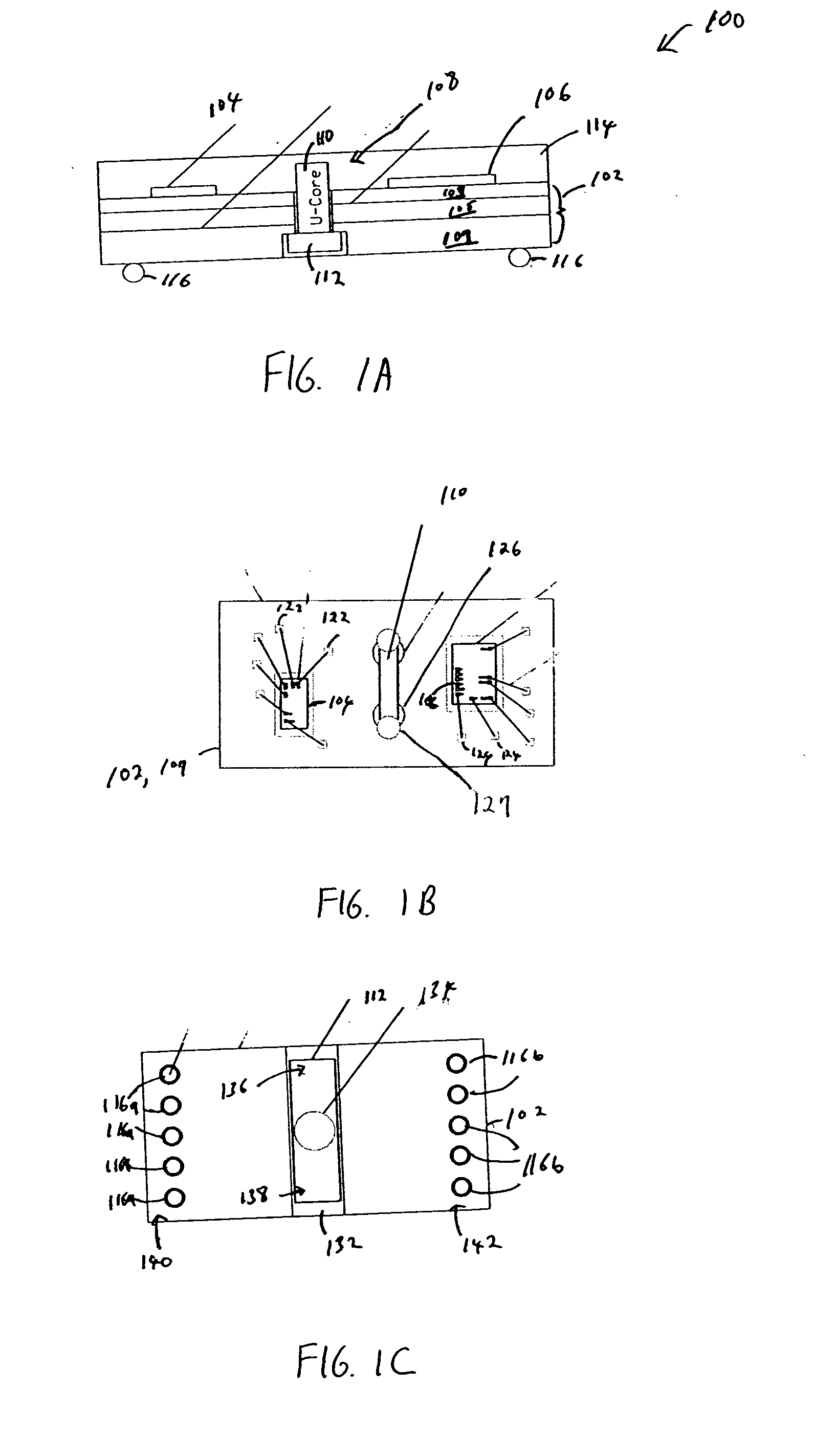
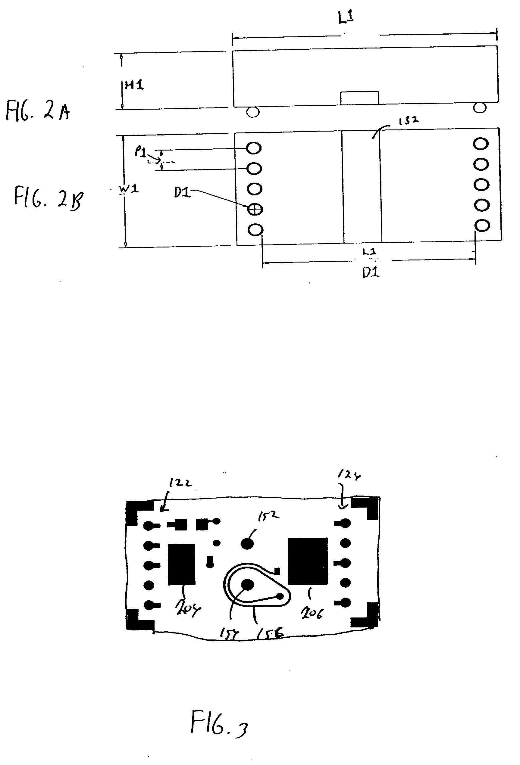
[0031] The present invention relates to a packaged device having one or more magnetic components. The packaged device may include one or more semiconductor or electrical components, e.g., die, resistor, and capacitor. The packaged device may be a power device (e.g., DC-DC converter), electronic device (e.g., gate driver), or electrical device (e.g., transformer or inductor). The magnetic components or ferrites are integrated into the packaged device using standard semiconductor package technologies. The magnetic component(s) may define a transformer or inductor according to application.

[0032] The packaged device is an isolated gate driver according to one embodiment of the present invention. The packaged power device includes various types of packaged devices, e.g., a ball grid array (BGA) and a plastic dual in-line package (PDIP). The present invention may be applied to many different types of devices, e.g., a gate driver, a DC-DC converter, and a power amplifier. These devices ma...


PUM


Abstract

A packaged device is obtained using an innovative package approach that allows integration of miniature planar magnetics into standard low-cost semiconductor packages (BGA, PDIP, SOIC, etc.) with electronic and electrical components, where those components can be C&W and / or SMD types. The packaged device includes a planar magnetic substrate having first and second dielectric layers, the first dielectric layer having a first winding defined thereon, the second dielectric layer having a second winding defined thereon. A magnetic component is provided in the substrate. A package material provided at least partly around the substrate and the magnetic component to protect the substrate and magnetic component. The magnetic component is an inductor or transformer. The packaged device further includes at least one semiconductor component provided on the first dielectric layer.

Description

CROSS-REFERENCES TO RELATED APPLICATIONS [0001] The present application claims priority to U.S. Provisional Patent Application No. 60 / 642,890, filed on Jan. 10, 2005, which is incorporated by reference.BACKGROUND OF THE INVENTION [0002] The present invention relates to a packaged device that integrates one or more magnetic components into standard semiconductor package technologies. The packed device may include one or more magnetic components only, or one or more magnetic components plus one or more electrical or electronic components, e.g., a semiconductor chip, resistor, or capacitor. [0003] Semiconductor power devices of various types are used in electronic and electrical parts to operate them. For example, power MOSFETs or IGBTs are used to supply power to electronic or electrical parts. These power MOSFETs and IGBTs, in turn, are commonly driven by gate drivers that are coupled to the gates of the power MOSFETs and IGBTs. [0004] The potential difference between the input side ...

Claims


Application Information

Patent Timeline
IPC IPC(8): H05K7/06
CPCH01F27/2804H01F27/292H01F2019/085H01L23/3128H01L23/49822H01L23/50H01L25/16H01L2224/48227H01L2224/48235H01L2924/13055H01L2924/13091H01L2924/15311H01L2924/19041H01L2924/19105H05K1/165H01L24/48H01L2924/14H01L2924/00014H01L2924/00H01L2224/45099H01L2224/45015H01L2924/207
Inventor HUMBERT, DONALDFURNIVAL, COURTNEY R.
Owner LITTELFUSE INC
Learn More