
Semiconductor device, wiring substrate, and method for manufacturing wiring substrate

a semiconductor device and wiring substrate technology, applied in the direction of individual semiconductor device testing, semiconductor/solid-state device testing/measurement, instruments, etc., can solve the problem of thermal stress concentration due to the difference of expansion coefficient, large internal stress within the semiconductor apparatus, and predicted to become difficult to maintain reliability. problem, to achieve the effect of reducing the mismatch of thermal expansion coefficient between them, reducing internal stress allowance level, and increasing reliability

Active Publication Date: 2006-07-13
GK BRIDGE 1
View PDF4 Cites 46 Cited by
  • Summary
  • Abstract
  • Description
  • Claims
  • Application Information

AI Technical Summary

Benefits of technology

[0011] It is another object of the present invention to provide a semiconductor apparatus, in which an internal stress caused by the difference of thermal expansion coefficients in a wiring substrate is decreased, thereby increasing the reliability and capable of responding to further shrinkage and pin-multiplication.
[0039] Furthermore, by stacking the wiring layer on the base substrate which has a small thermal expansion coefficient and a high rigidity, it becomes possible to form a fine wiring pattern compared with the case where the wiring layer is stacked on a resin-based base material.

Problems solved by technology

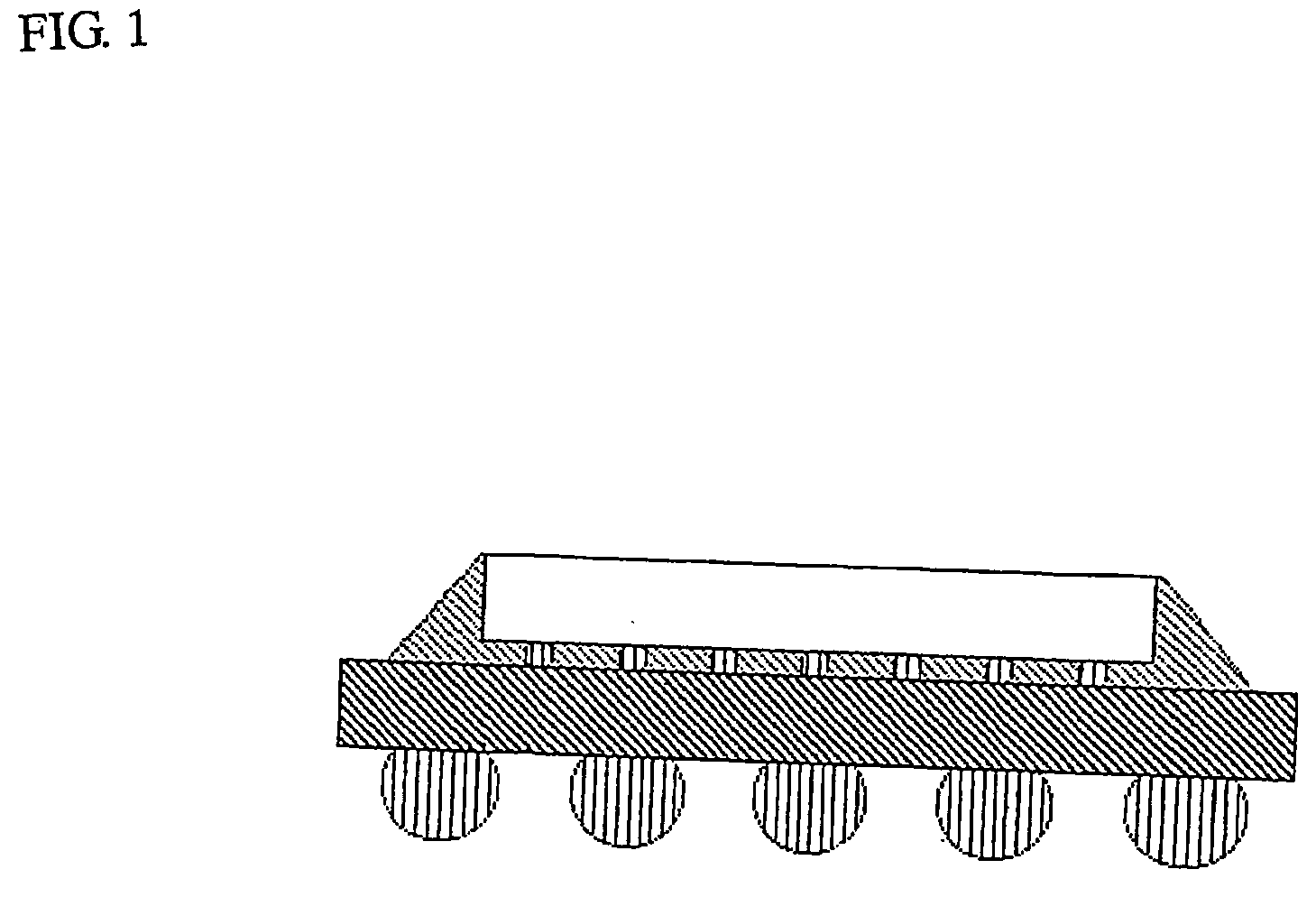
The difference is large, thereby causing a large internal stress within the semiconductor apparatus by the difference of thermal expansion coefficient between them.
However, by increase in internal stress due to growing in size of semiconductor chip according to increase of the number of external terminal in a future, it is predicted to become difficult to maintain the reliability.
Then, the issue of thermal stress concentration due to the difference of the expansion coefficient has not been solved.
Then, it is well known that the Low-k film is fragile compared with a conventional interlayer dielectric film such as silicon oxide film.
This means a decrease in allowable limit of the internal stress caused by the difference of linear expansion coefficient between the semiconductor chip and the interposer substrate, and may cause a reliability issue when the shrinkage and pin-multiplication are further progressed in a future.
Accordingly, the internal stress increases, and may cause a reliability issue when the shrinkage and pin-multiplication are further progressed in a future.

Method used


Image

  • Semiconductor device, wiring substrate, and method for manufacturing wiring substrate
  • Semiconductor device, wiring substrate, and method for manufacturing wiring substrate
  • Semiconductor device, wiring substrate, and method for manufacturing wiring substrate

Examples


first embodiment

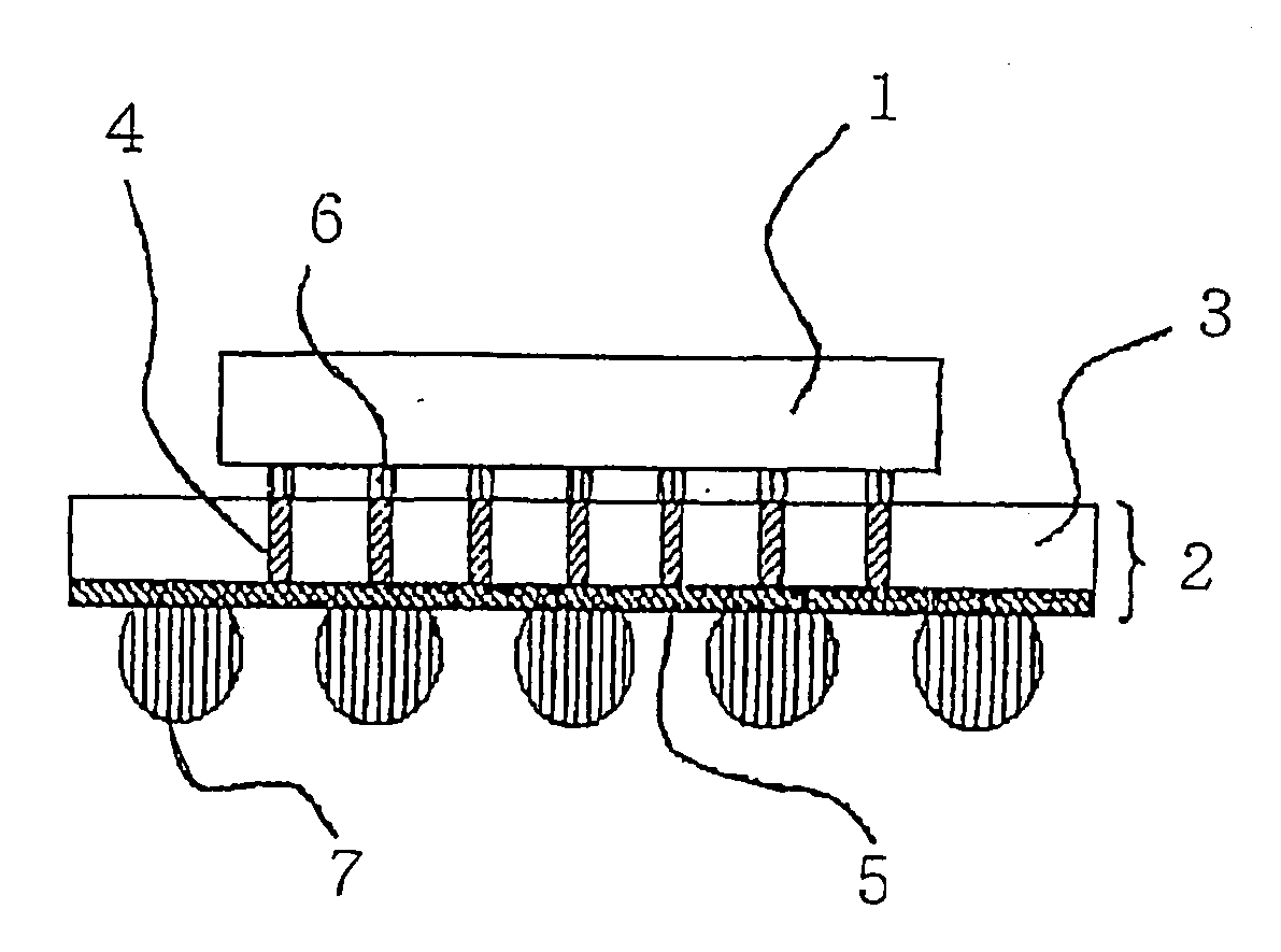
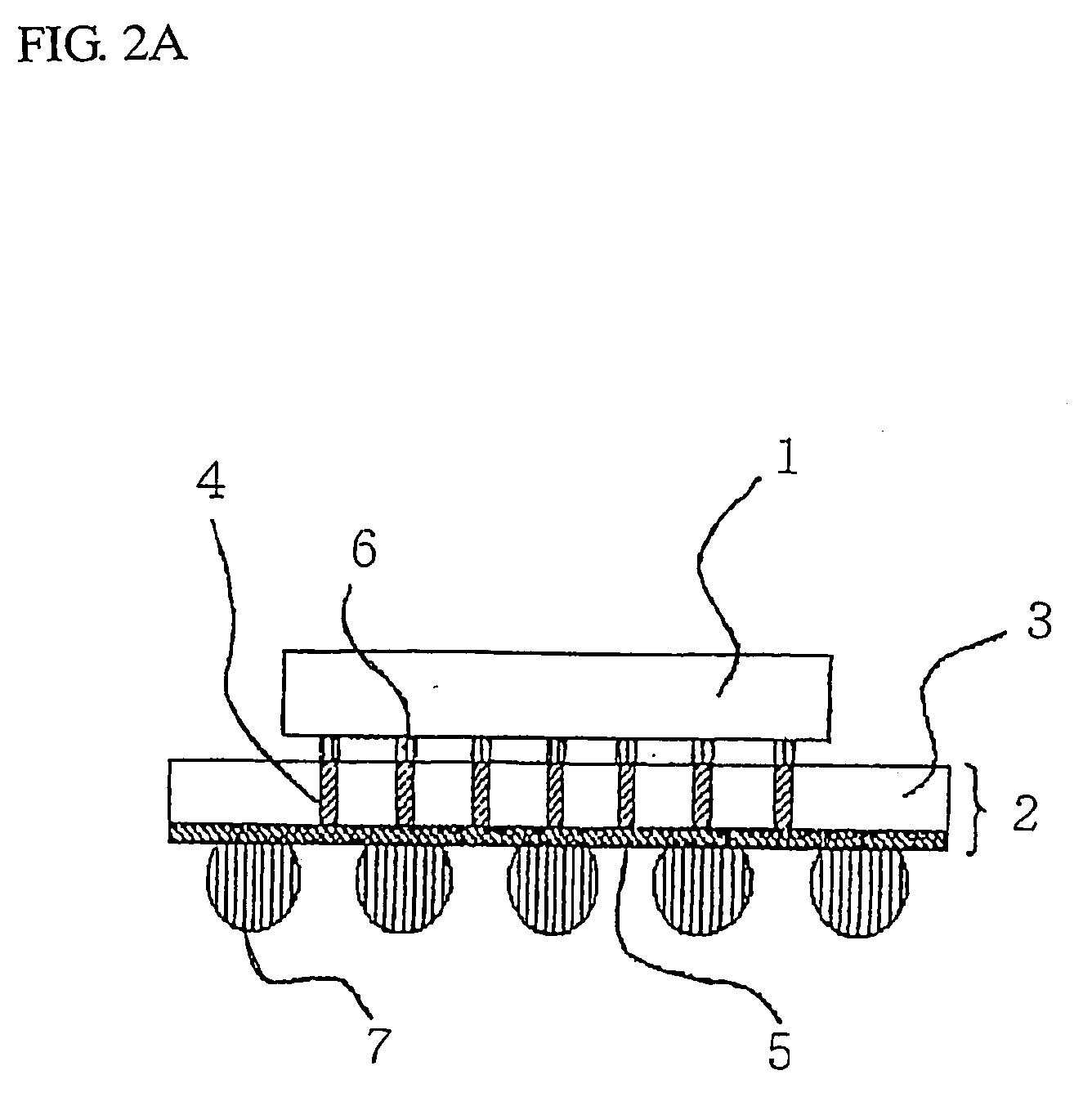
[0049] Embodiments of the present invention will be explained in detail by referring to figures. FIG. 2A is a cross sectional view showing a structure of a first example of a semiconductor apparatus in the first embodiment of the present invention. FIG. 2B is a cross sectional view showing a structure of a second example of a semiconductor apparatus in the first embodiment of the present invention. FIG. 2C is a cross sectional view showing a structure of a third example of a semiconductor apparatus in the first embodiment of the present invention. FIGS. 3A to 3F are cross sectional views of a wiring substrate at each process of a method for manufacturing the wiring substrate of the semiconductor apparatus in the first embodiment of the present invention.

[0050] In the first embodiment, as shown in FIG. 2A, a single or plural wiring layers 5 is formed on one side of base substrate 3 which is composed of silicon as a wiring substrate 2, and on an electrode at the top layer of wiring l...

second embodiment

[0066]FIG. 4 is a cross sectional view showing a structure of semiconductor apparatus in the second embodiment of the present invention. In the second embodiment, in addition to the configuration of the first embodiment, a stiffener 9 of reinforcing frame is stuck at around a mounting surface area of semiconductor chip 1 on base substrate 3 for increasing rigidity of wiring substrate 2. Since the rigidity of wiring substrate 2 can be increased with stiffener 9, it is possible to thin the thickness of a package by thinning base substrate 3, and to provide countermeasures for increasing cooling performance against the increase of power consumption and heat generation of semiconductor chip 1 by attaching heat sink 10 at the bottom of semiconductor chip 1 using stiffener 9. It is also favorable that a thermal expansion coefficient of stiffener 9 is equal to that of semiconductor chip 1, or less than that of wiring layer 5, as well as the case of base substrate 3.

third embodiment

[0067]FIG. 5A to 5E are cross sectional views of a wiring substrate at each process of a method for manufacturing a wiring substrate of a semiconductor apparatus in a third embodiment of the present invention.

[0068] In the first embodiment, wiring layer 5 is formed after forming a half-through-hole in base substrate 3, and burying the half-through-hole with an electrically conductive material. However, in the third embodiment, after forming wiring layer 5 first on base substrate 3, wiring substrate 2 is completed by forming a through-electrode and a backside electrode

[0069] First, as shown in FIG. 5A, insulating layer 11a and wiring layer 5 are formed on base substrate 3 of silicon having a thickness of 700 μm with the same manufacturing method as the first embodiment.

[0070] After protecting a surface of wiring layer 5 with support 17, the wafer is turned over and base substrate 3 is thinned to 180 μm from backside with mechanical grinding. Then, a central part of base substrate ...


PUM


Abstract

The reliabilities of a wiring substrate and a semiconductor apparatus are improved by reducing the internal stress caused by the difference of thermal expansion coefficients between a base substrate and a semiconductor chip. A wiring layer (5) is provided on one surface of a silicon base (3). An electrode as the uppermost layer of the wiring layer (5) is provided with an external bonding bump (7). A through-electrode (4) is formed in the base (3) for electrically connecting the wiring layer (5) and an electrode terminal. The electrode terminal on the chip mounting surface is bonded to an electrode terminal of a semiconductor chip (1) by an internal bonding bump (6). The thermal expansion coefficient of the silicon base (3) is equivalent to that of the semiconductor chip (1) and not more than that of the wiring layer (5).

Description

FIELD OF THE INVENTION [0001] The present invention relates to a semiconductor apparatus, a wiring substrate for the semiconductor apparatus and a method for manufacturing the wiring substrate, and, more particularly to a Flip-Chip type semiconductor apparatus which is a face-down type, the wiring substrate for the Flip-Chip type semiconductor apparatus and a manufacturing method for the wiring substrate. BACKGROUND OF THE INVENTION [0002] All of patents, patent applications, patent publications, scientific articles and the like, which will hereinafter be cited or identified in the present application, will hereby be incorporated by references in their entirety in order to describe more fully the state of the art, to which the present invention pertains. [0003] Recently, for improving mounting density of a semiconductor package, shrinkage, miniaturization, and pin-multiplication of the package has been progressed. Aligning electrode terminal in the area is an effective technology ag...

Claims


Application Information

Patent Timeline
IPC IPC(8): H01L23/12H01L21/58H01L23/14
CPCH01L23/147H01L2924/09701H01L2924/12044H01L2224/16225H01L2224/32225H01L2224/73204H01L2924/15311H01L2924/00H01L2224/45144H01L2224/16235H01L2924/18161
Inventor NISHIYAMA, TOMOHIROTAGO, MASAMOTO
Owner GK BRIDGE 1
Learn More