
Gallium nitride semiconductor and method of manufacturing the same

a technology of gallium nitride and semiconductor, applied in the direction of polycrystalline material growth, crystal growth process, chemistry apparatus and processes, etc., can solve the problems of compressive strain, large differences in lattice parameters and thermal expansion coefficients between, and difficulty in growing high-quality nitride semiconductor thin films, etc., to improve performance and reliability, reduce crystal defects

Active Publication Date: 2006-07-06
LG SILTRON
View PDF9 Cites 6 Cited by
  • Summary
  • Abstract
  • Description
  • Claims
  • Application Information

AI Technical Summary

Benefits of technology

[0012] The present invention is conceived to solve the aforementioned problems in the prior art, including the need to provide a GaN semiconductor and a method of manufacturing the same, which can reduce crystal defects caused by differences in lattice parameter and thermal expansion coefficient between a GaN semiconductor thin film and a substrate, thereby improving performance and reliability of the semiconductor.

Problems solved by technology

However, there hardly exists a substrate that is lattice matched with this GaN semiconductor, and differences in lattice parameters and thermal expansion coefficients therebetween are too large.
Therefore, it is very difficult to grow a high-quality nitride semiconductor thin film.
However, when GaN grows on actual (0001) sapphire, an effective lattice parameter of sapphire is smaller than that of GaN by about 14%, which causes a compressive strain.
Moreover, since lattice defects having large threading dislocation density of about 1014 / cm2 are caused, it is difficult to achieve the growth of a high-quality single crystal.
In addition, since a crack can be caused when the thickness exceeds 10 μm, it is difficult to grow a high-quality GaN thin film layer, and the life and characteristic efficiency of devices made therefrom can also be reduced.
Nevertheless, when the buffer layer for the heteroepitaxy is grown to about 1 to 500 nm, and the GaN thin film grows on the grown buffer layer, the buffer layer includes crystal defects due to differences in thermal expansion coefficients and lattice parameters of the substrate and buffer layer.
As a result, the large number of crystal defects make it difficult to form a high-quality GaN thin film.
This manufacturing preference has a negative impact on the productivity of manufacturing LEDs or LDs in large quantities.
Therefore, for a device manufactured using 2 sapphire substrate, the back ohmic contact cannot be easily formed, as compared with other devices manufactured using conductive substrates.
Accordingly, an additional process or post-process is required for forming electrodes while manufacturing the device, which increases the complexity of the overall manufacturing process.
As a result, manufacturing costs are increased, and the performance of devices can be degraded due to the increased serial resistance of the device.
However, SiC is more expensive than sapphire, and the performance of the GaN device using a SiC substrate is reported to be inferior to that using a sapphire substrate.
Although substantial research has been conducted on the growth of the GaN thin film using a silicon substrate as an alternative to sapphire or SiC substrates there remain problems due to the differences in the lattice parameters and thermal expansion coefficients occurring in the conventional sapphire and SiC substrates.
However, the silicon substrate still has problems to be solved if more stable devices having reproducible characteristics are to be produced.

Method used


Image

  • Gallium nitride semiconductor and method of manufacturing the same
  • Gallium nitride semiconductor and method of manufacturing the same
  • Gallium nitride semiconductor and method of manufacturing the same

Examples


Embodiment Construction

[0025] Hereinafter, a GaN semiconductor and a method of manufacturing the same according to a preferred embodiment of the present invention will be described in detail with reference to the accompanying drawings.

[0026] In the present invention, a (111) plane of silicon is used as a growth substrate of a GaN semiconductor. The theoretical lattice parameter of the a-axis of silicon is 5.42 Å. When a (100) plane of silicon is used as a growth substrate, the silicon has an advantage in that its chemical characteristics are stable and its electric characteristics are long-lasting, but (100) silicon has a significantly great lattice mismatch, as compared with GaN which has a lattice parameter of 3.186 Å. However, if a (111) plane is used, the theoretical lattice parameter of silicon becomes 3.83 Å, and thus, the lattice mismatch with the GaN semiconductor can be drastically reduced.

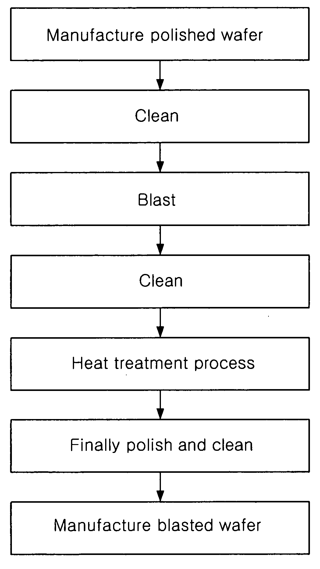
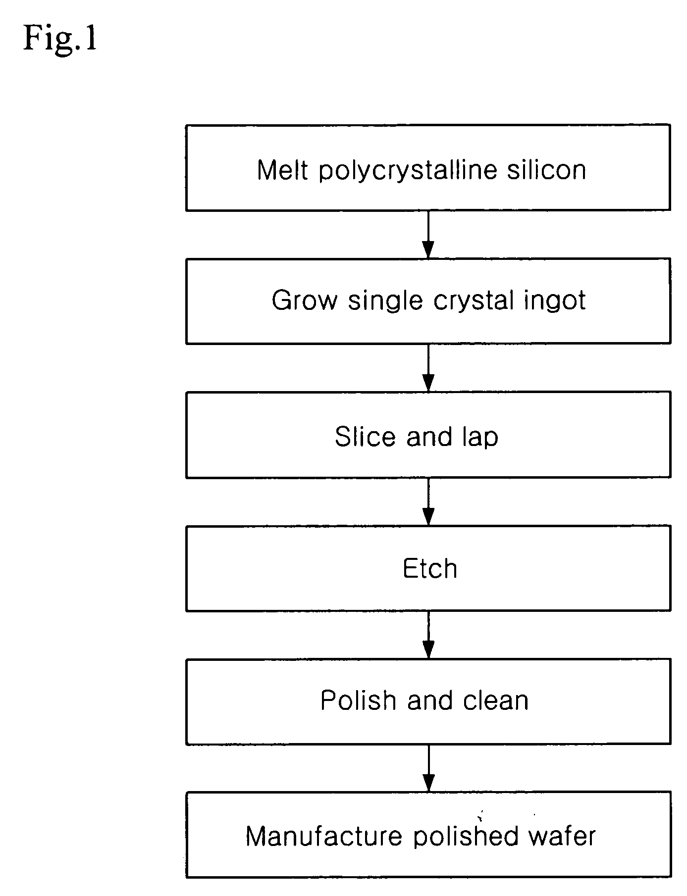
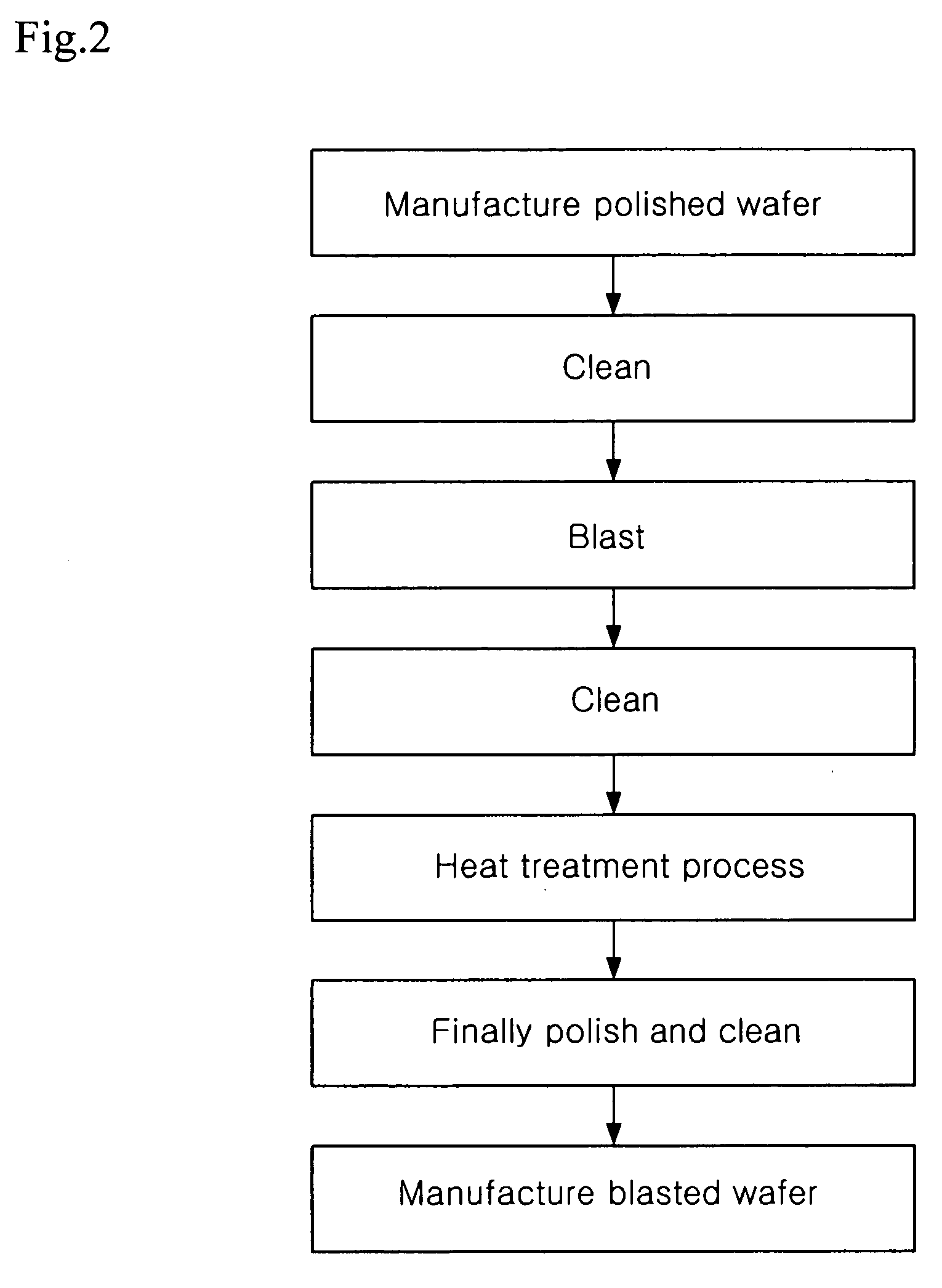
[0027]FIG. 1 is a flowchart showing a general process of manufacturing a polished wafer.

[0028] First, pol...


PUM


Abstract

The present invention provides to a gallium nitride (GaN) semiconductor and a method of manufacturing the same, capable of reducing crystal defects caused by a difference in lattice parameters, and minimizing internal residual stress. In particular, since a high-quality GaN thin film is formed on a silicon wafer, manufacturing costs can be reduced by securing high-quality wafers with a large diameter at a low price, and applicability to a variety of devices and circuit can also be improved.

Description

CROSS-REFERENCE TO RELATED APPLICATION [0001] This application claims priority of Korean Patent Application No. 10-2004-0105371 filed Dec. 14, 2004, the entire disclosure of which is incorporated by reference herein. FIELD OF THE INVENTION [0002] The present invention relates to a gallium nitride (GaN) semiconductor having an improved GaN thin film and a method of manufacturing the same. BACKGROUND OF THE INVENTION [0003] GaN has a direct bandgap of 3.4 eV at room temperature and, if combined with indium nitride (InN) or aluminum nitride (AlN), can have a direct bandgap of 1.9 eV (InN) or 6.2 eV (AlN). Due to its wide wavelength range spanning the visible light to ultraviolet regions of the electromagnetic spectrum, GaN is a desirable material for light-emitting element applications. Since the material's emission wavelength can be controlled over a wide range, GaN can be used to make light-emitting elements capable of emitting over a wide spectrum of visible light. Consequently, the...

Claims


Application Information

Patent Timeline
IPC IPC(8): H01L31/109H01L29/12H01L33/12H01L33/32
CPCC30B29/406H01L21/02381H01L21/0243H01L21/02439H01L21/0254H01L21/02658
Inventor KIM, YONG JINLEE, DONG KUN
Owner LG SILTRON
Learn More