A CMOS imager with cu wiring and method of eliminating high reflectivity interfaces therefrom
a technology of cmos and imager, applied in the field of cmos (complementary metal oxide semiconductor) image sensor array structure, can solve problems such as degrading device sensitivity
- Summary
- Abstract
- Description
- Claims
- Application Information
AI Technical Summary
Benefits of technology
Problems solved by technology
Method used
Image
Examples
first embodiment
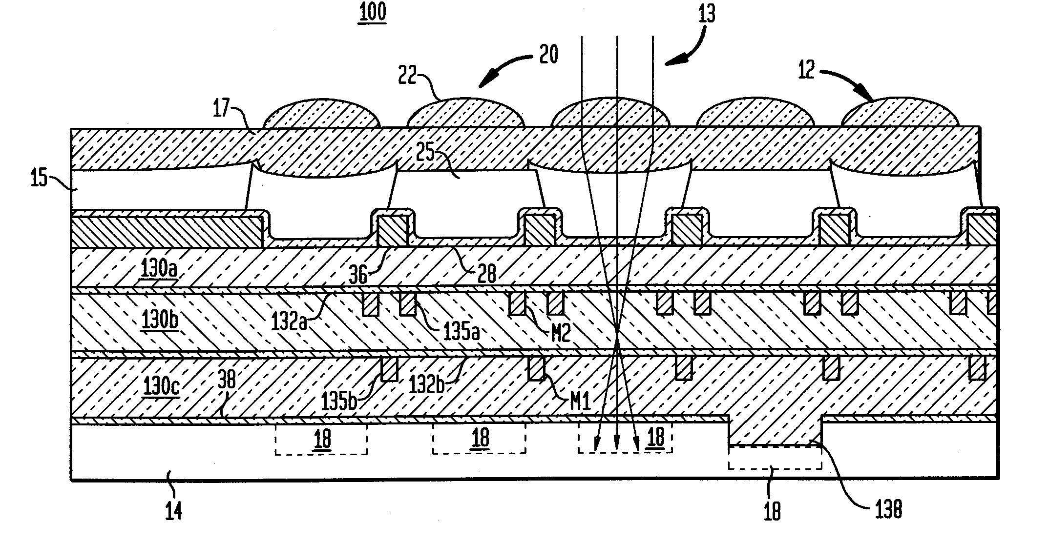
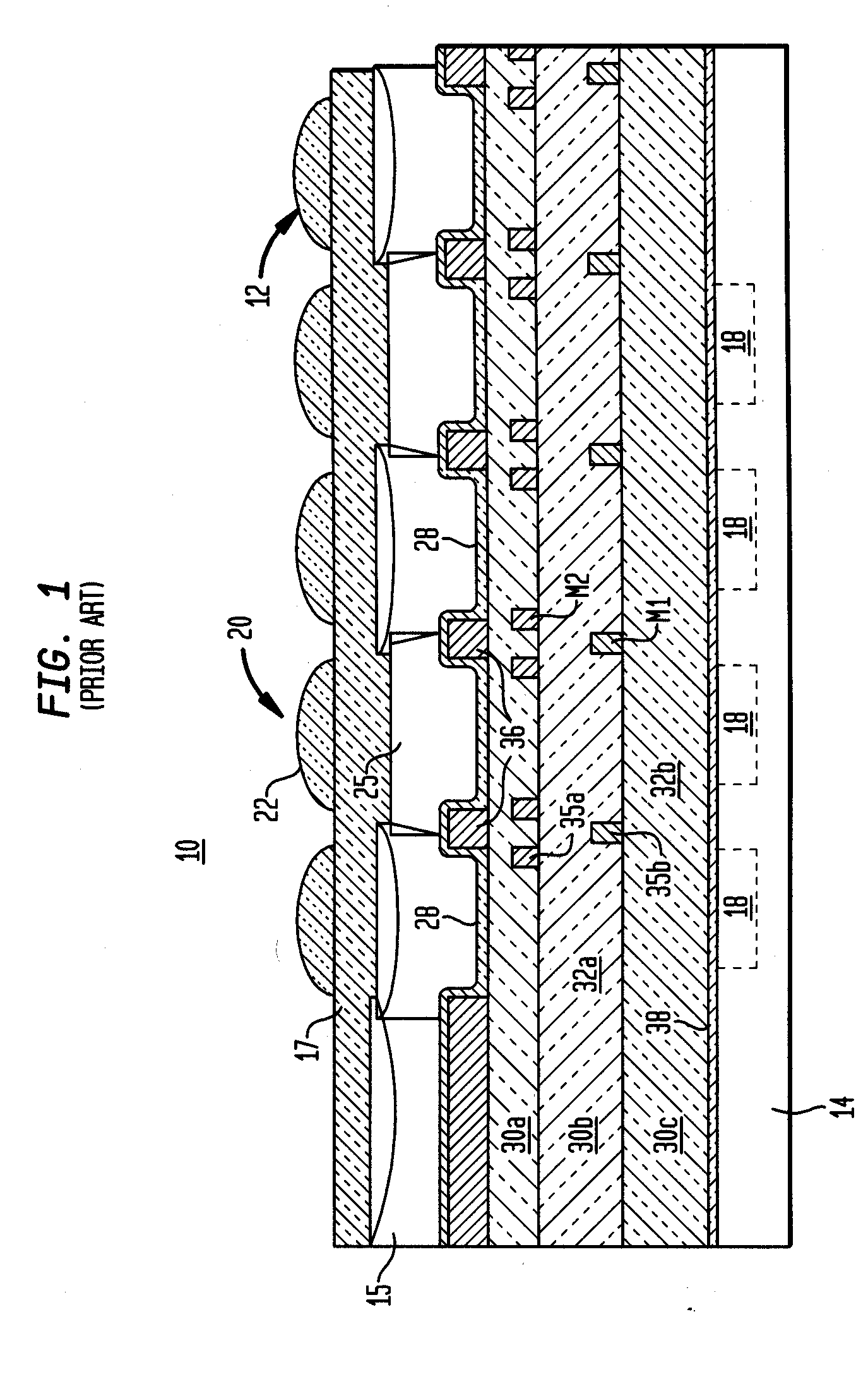
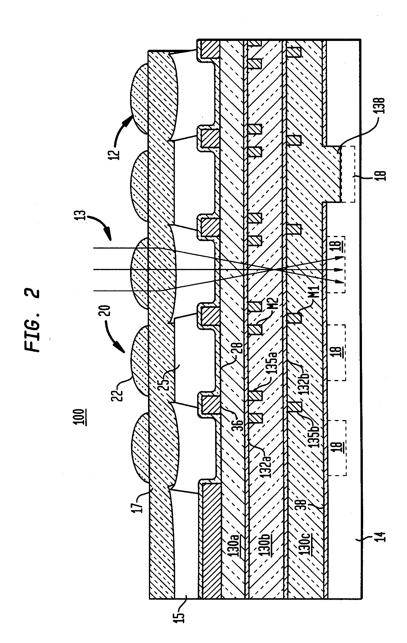
[0043]FIG. 2 illustrates, through a cross-sectional view, a back end of line image sensor array stack 100 according to the invention. While the upper light receiving portion of the pixels 20 (microlens and color filters) are the same as the prior art depicted in FIG. 1, the invention includes the formation of Cu metallization interconnects M1, M2 allowing for the formation of thinner stack of interlevel dielectric layers 130a-130c formed on the substrate 14. The substrate 14 may be a bulk semiconductor including, for example, Si, SiGe, SiC, SiGeC, GaAs, InP, InAs and other III-V compound semiconductors, II-V compound semiconductors, or layered semiconductors such as silicon-on-insulators (SOI), SiC-on-insulator (SiCOI) or silicon germanium-on-insulators (SGOI). Preferably, the interlevel dielectric material may comprise an organic or inorganic interlevel dielectric (ILD) material which may be deposited by any of number of well known techniques such as sputtering, spin-on, or PECVD a...
second embodiment
[0046] Thus, in an alternate second embodiment of pixel array 100b depicted in FIG. 3(b), for the embodiment including STI isolation dielectric regions 138 formed on top of the light sensitive element, e.g., photodiode 18, it is advantageous to remove the substrate capping layer 38 in the optical path on top of the substrate 14 image sensor array 100a in addition to the M1 and M2 level dielectrics 132a,b in the optical path. Thus, in the manner described herein with respect to FIG. 3(a), an additional mask is required and additional lithographic patterning and etching steps (wet or dry etch) implemented to provide additional openings 50a in the SiN capping layer 38 at the locations of the pixel's optical path.
third embodiment
[0047]FIG. 4(a) illustrates, through a cross-sectional view, the image sensor array 100c according to the invention which corresponds to the image sensor embodiment depicted in FIG. 3(a) without the STI regions 138 above the pixel's light sensitive element (photodiode) 18 in the substrate 14. According to this embodiment, the substrate capping layer 38, interlevel dielectric layer 130a, interlevel metallization 135b (M1) and corresponding barrier layer 132b, e.g., SiN, are formed without the M1 barrier etching. Then, the M2 dielectric layer 130b, metallization M2135a and corresponding barrier layer 132a, e.g., SiN, are formed. A mask is subsequently patterned and an etch is conducted to create an opening 51 to remove that portion of the Nitride barriers 132a for the M2 layer from the pixels' optical paths. However, in the same etch process step, the M2 dielectric layer 130b and the M1 barrier opening 51a is created so that the only one mask is needed to remove both metallization bar...
PUM
 Abstract
Description
Claims
Application Information
 - R&D
- Intellectual Property
- Life Sciences
- Materials
- Tech Scout
- Unparalleled Data Quality
- Higher Quality Content
- 60% Fewer Hallucinations
Browse by: Latest US Patents, China's latest patents, Technical Efficacy Thesaurus, Application Domain, Technology Topic, Popular Technical Reports.
© 2025 PatSnap. All rights reserved.Legal|Privacy policy|Modern Slavery Act Transparency Statement|Sitemap|About US| Contact US: help@patsnap.com


