
Semiconductor substrate and its fabrication method

a technology of semiconductors and substrates, applied in the direction of optical elements, instruments, optical waveguide light guides, etc., can solve the problems of large cost of forming methods, inability to obtain sufficient reliability, and inability to meet the requirements of household electronic devices such as drams, so as to achieve the effect of not raising costs or deteriorating reliability

Inactive Publication Date: 2006-06-22
KK TOSHIBA
View PDF10 Cites 72 Cited by
  • Summary
  • Abstract
  • Description
  • Claims
  • Application Information

AI Technical Summary

Benefits of technology

The present invention provides a semiconductor substrate and fabrication method that have a similar effect to an SOI structure without increasing cost or compromising reliability. The substrate has a flat empty space or a flat insulating member that serves as an insulator and provides an ideal SOI structure. The empty space can be formed by forming trenches on the substrate and then heating the substrate to change the trenches to one flat empty space. The fabrication method involves forming a plurality of trenches on the substrate, filling the empty spaces with insulating films, and optionally forming an oxide film on the inner face of the empty space. The semiconductor substrate can be a silicon substrate, and the heat treatment can be performed at a reduced pressure in an atmosphere of SiO2 or a hydrogen atmosphere. The invention allows for the formation of an SOI structure only in the necessary regions, reducing cost and improving device design flexibility. The method also prevents deterioration of reliability by minimizing surface migration and improving crystallinity. The invention also allows for the use of a silicon substrate with defects, reducing the cost of the wafer.

Problems solved by technology

However, because a conventional SOI-substrate forming method requires a large cost, there is a problem that an SOI substrate is not suitable for a household electronic device such as a DRAM.
Moreover, because it is difficult to form a silicon region (element-forming region) having less defects, there is also a problem that a sufficient reliability cannot be obtained compared to the case of using a bulk silicon substrate.

Method used


Image

  • Semiconductor substrate and its fabrication method
  • Semiconductor substrate and its fabrication method
  • Semiconductor substrate and its fabrication method

Examples


first embodiment

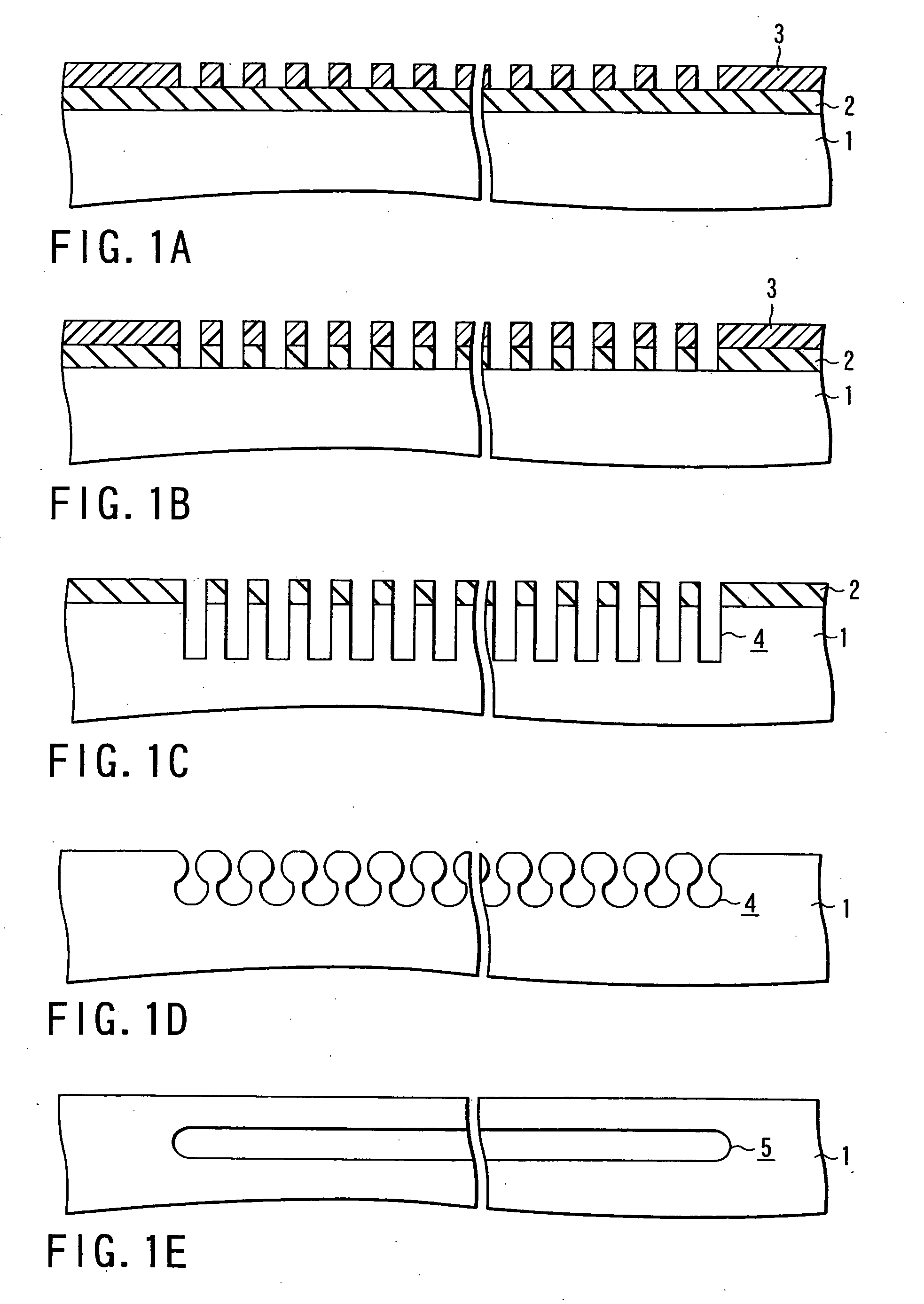
[0072]FIGS. 1A to 1E are sectional views showing a method for fabricating a silicon substrate having a flat empty space (ESS: Empty Space in Silicon) of the first embodiment of the present invention, that is, an SON (Silicon On Nothing) substrate referred to as an ultimate SOI substrate.

[0073] First, as shown in FIG. 1A, a mask material 2 is formed on a single-crystal silicon substrate 1 and a photoresist pattern 3 is formed on the mask-material 2. The mask material 2 will be described later.

[0074] Then, as shown in FIG. 1B, the mask material 2 is patterned through anisotropic etching such as RIE by using the photoresist pattern 3 as a mask to transfer the pattern of the photoresist pattern 3 to the mask material 2.

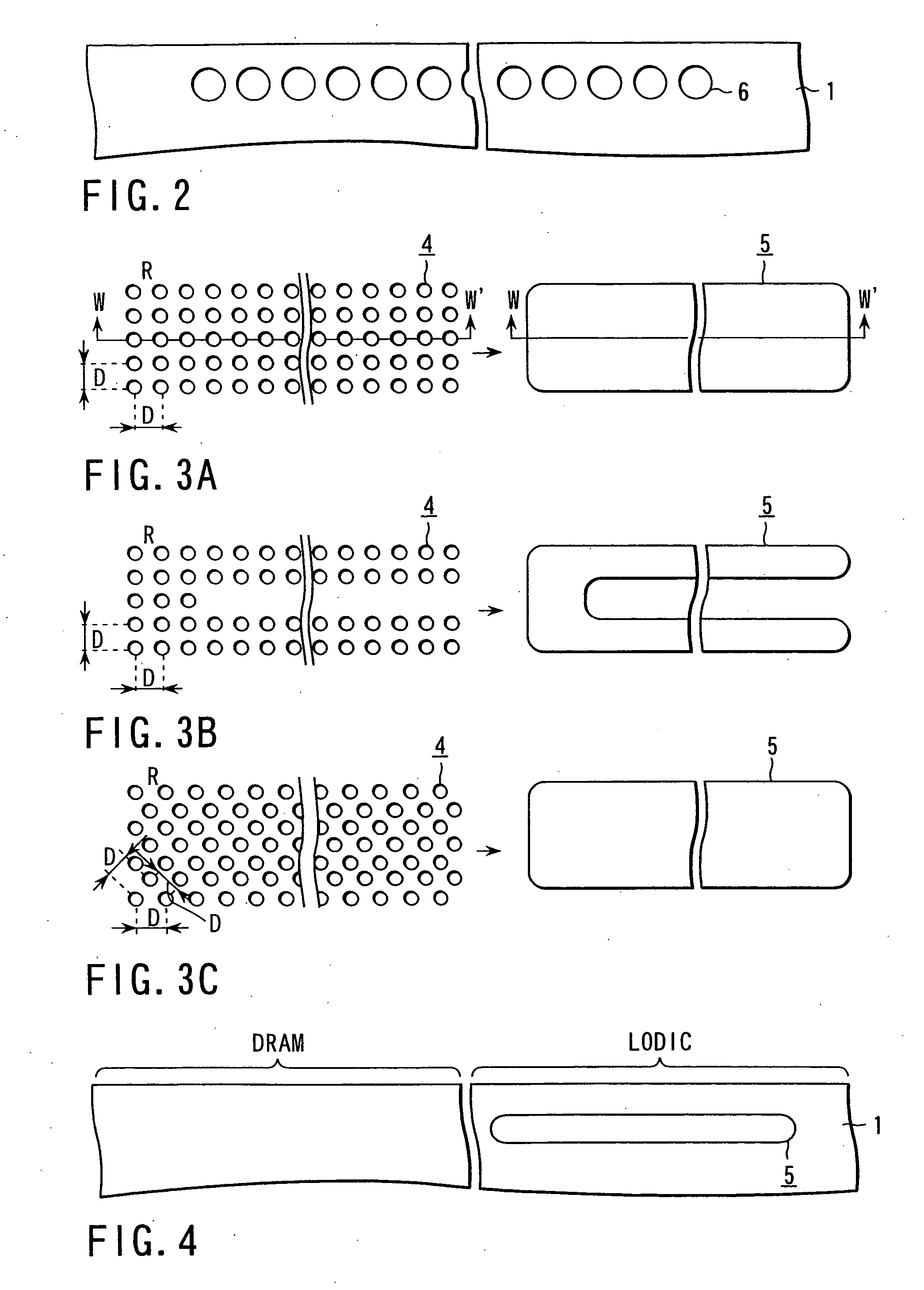
[0075] Then, as shown in FIG. 1C, the photoresist pattern 3 is carbonized and separated and then, the silicon substrate is patterned through anisotropic etching such as RIE by using the mask material 2 as a mask to two-dimensionally arrange a plurality of trenches 4 on...

second embodiment

[0103]FIGS. 5A to 5L are sectional views showing a method for fabricating a MOS transistor of the second embodiment of the present invention. In the following drawings, a symbol same as that in a previous drawing shows the same or a corresponding portion and its detailed description is omitted.

[0104] For this embodiment, a case is described in which a flat empty space is formed in a silicon substrate to fabricate a MOS transistor on the flat empty space.

[0105] First, a flat empty space 5 is formed in a silicon substrate 1 as shown in FIG. 5A in accordance with the same method as the case of the first embodiment shown in FIGS. 1A to 1E.

[0106] Then, as shown in FIG. 5B, a silicon oxide film 7, a silicon nitride film 8, and a photoresist pattern 9 are formed in order on the silicon substrate 1.

[0107] In this case, the photoresist pattern 9 is laid out so that at lest a part of the opening of the pattern 9 is brought onto an empty space forming region. FIG. 5B shows a case in which ...

third embodiment

[0127]FIGS. 6A to 6D are sectional views showing a method for fabricating a MOST transistor of the third embodiment of the present invention. For the second embodiment, a method for filling a flat empty space with a silicon oxide film is described. For the third embodiment, however, a method for leaving a flat empty space without filling the empty space with a silicon oxide film is described.

[0128] First, as shown in FIG. 6A, a flat empty space 5 is formed in a silicon substrate 1 in accordance with the method used for the first embodiment shown in FIGS. 1A to 1E.

[0129] Then, as shown in FIG. 6B, a silicon thermal oxide film 24 is formed in the flat empty space 5 and on the surface of the silicon substrate through thermal oxidation. The above thermal oxidation is performed, for example, in a mixed gas of oxygen and HCl at 900° C. A silicon thermal oxide film 22 serves as a stopper under RIE as shown in FIG. 5G in subsequent steps.

[0130] Then, as shown in FIG. 6C, a silicon nitrid...


PUM


Abstract

To change a plurality of trenches to one flat empty space by two-dimensionally forming the trenches on the surface of a semiconductor substrate and then applying heat treatment to the semiconductor substrate.

Description

CROSS-REFERENCE TO RELATED APPLICATIONS [0001] This application is based upon and claims the benefit of priority from the prior Japanese Patent Applications No. 11-246582, filed Aug. 31, 1999; and No. 2000-252881, filed Aug. 23, 2000, the entire contents of which are incorporated herein by reference. BACKGROUND OF THE INVENTION [0002] More operational speedup and power saving have been recently requested for electronic devices including a DRAM. As one of means for realizing operational speedup and power saving, it is listed to use SOI (Silicon On Insulator) substrate instead of a silicon substrate (bulk silicon substrate) normally used. [0003] An SOI substrate is a substrate having a structure that a silicon region is present on an insulating region and there are several types of SOI-substrate forming methods such as the bonding method, SIMOX (Separator by IMplanted OXygen) method, and ELTRAN (Epitaxial Layer TRANsfer) method. [0004] However, because a conventional SOI-substrate for...

Claims


Application Information

Patent Timeline
Patent Type & Authority Applications(United States)
IPC IPC(8): H01L27/12G02B6/10G02B6/12G02B6/122H01L21/00H01L21/336H01L21/76H01L21/762H01L21/764H01L21/822H01L21/8238H01L21/84H01L27/04H01L27/08H01L27/092H01L27/10H01L29/06H01L29/78H01L29/786H01L29/84H10B12/00
CPCB82Y20/00G02B6/122G02B6/1225G02B2006/12097H01L21/3247H01L21/7624H01L21/76283H01L21/76289H01L21/764H01L21/84H01L27/10805H01L27/10894H01L27/10897H01L27/12H01L27/1203H01L29/0657H01L29/7842H01L29/78603H01L29/78639H10B12/30H10B12/50H10B12/09H01L29/78
Inventor SATO, TSUTOMUMATSUO, MIEMIZUSHIMA, ICHIROTSUNASHIMA, YOSHITAKATAKAGI, SHINICHI
Owner KK TOSHIBA
Learn More