
Schottky barrier diode

Inactive Publication Date: 2006-04-27
MITSUBISHI ELECTRIC CORP
View PDF7 Cites 54 Cited by
  • Summary
  • Abstract
  • Description
  • Claims
  • Application Information

AI Technical Summary

Benefits of technology

[0012] It is an object of the present invention to provide a Schottky barrier diode capable of reducing noise while achieving size reduction and cost reduction.
[0014] This reduces a series resistance component and a capacitance component, thereby to improve a conversion gain and reduce a noise figure with low LO power when a frequency conversion is performed in a mixer. In other words, the higher performance of the mixer is attained.

Problems solved by technology

It is, however, difficult for the HEMT to provide a sufficient low noise characteristic in a low intermediate frequency band because the HEMT generally has extremely high 1 / f noise.
It is, however, inappropriate to mount all of the devices on a Si substrate because the transmission line loss of the Si substrate is extremely high in the microwave and millimeter-wave bands.
Consequently, the Si-SBD mixer is not suitable for the size reduction and the cost reduction.
The provision of such an etching stopper layer creates a problem such that a deep level in AlGaAs near a Schottky interface induces the 1 / f noise.
There arises another problem such that the increase in series resistance component in the SBD decreases the conversion gain of the frequency conversion in the mixer using the SBD to increase the noise figure.
Japanese Patent Application Laid-Open No. 10-51012 discloses the effect of reducing a resistance by etching down into an n− GaAs layer, but does not disclose the effect of reducing noise.
This, however, presents a problem such that crystal defects are created in a GaAs substrate to induce noise when ion implantation is performed.
Another problem is such that the high-concentration ion-implanted region, which is higher in resistance than metal, results in the increase in noise figure.

Method used


Image

  • Schottky barrier diode
  • Schottky barrier diode
  • Schottky barrier diode

Examples


first preferred embodiment

[0025] A receiver mixer according to a first preferred embodiment of the present invention is characterized by the use of a GaAs-SBD (Schottky barrier diode) for purposes of size reduction and cost reduction and by the reduction in noise at an intermediate frequency in the GaAs-SBD.

[0026] In general, the noise figure NF of a mixer is expressed as: NF=Si / NiSo / No=NoGcNi(1)

where Si is input signal power, Ni is input noise power, So is output signal power, No is output noise power, and Gc is a conversion gain.

[0027] The input noise power Ni is a constant determined by temperature. Thus, Equation (1) shows that the noise figure NF depends on the output noise power No generated in the SBD and the conversion gain Gc.

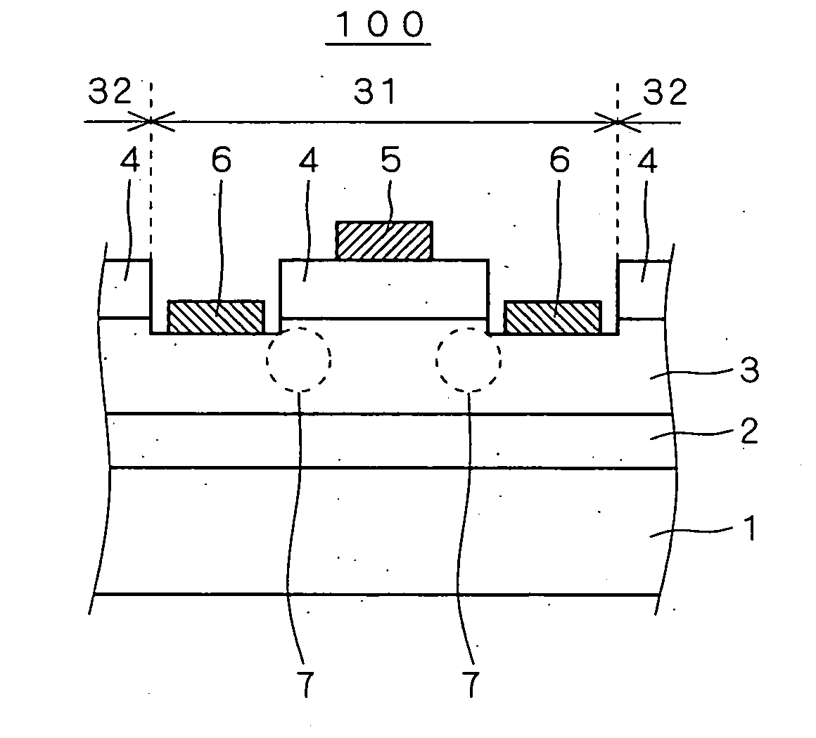
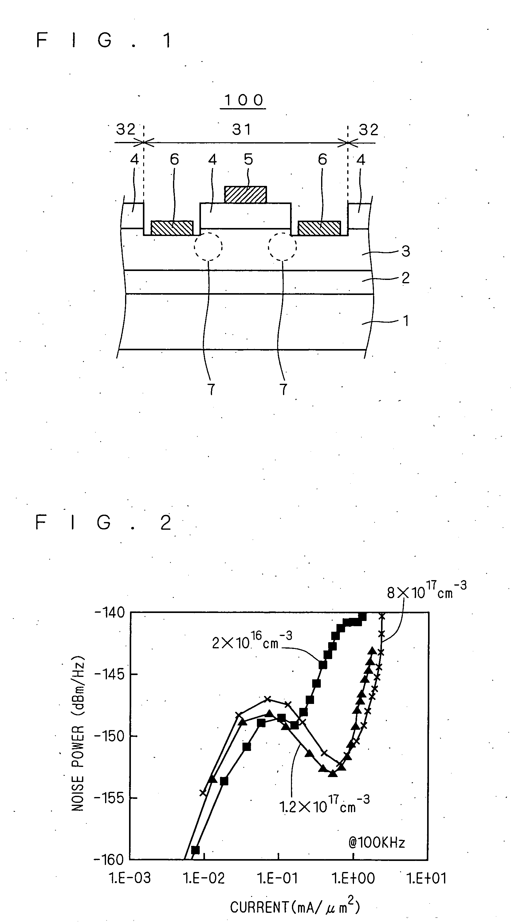
[0028]FIG. 1 is a sectional view showing a structure of principal parts of an SBD 100 according to the first preferred embodiment of the present invention. Parts which are not directly relevant to the present invention are not shown in FIG. 1.

[0029] With reference to FIG....


PUM


Abstract

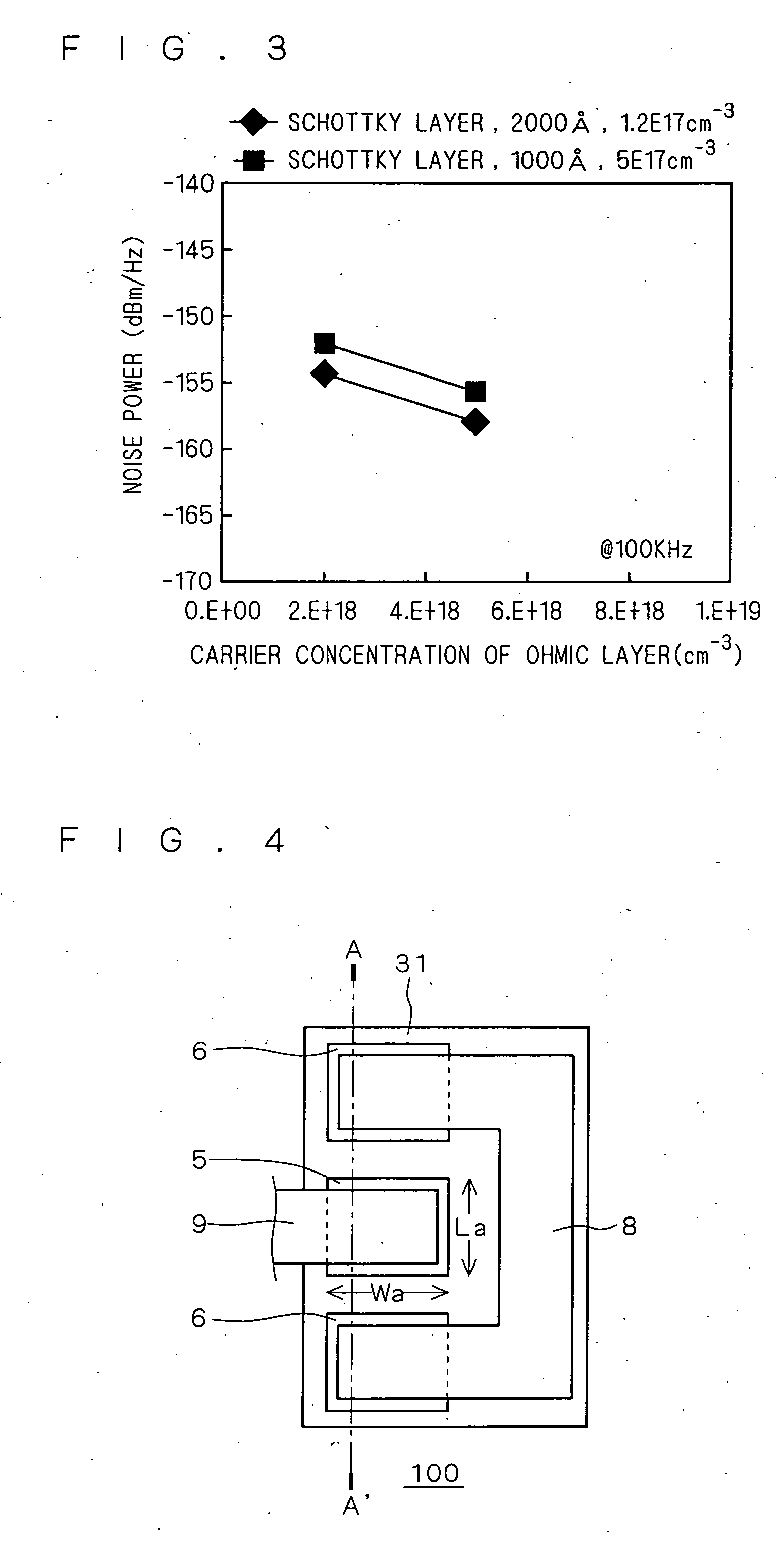
A buffer layer made of i-GaAs not doped with impurities, and an n+ GaAs layer doped with a high-concentration of n-type impurities are stacked in the order named on a semi-insulating GaAs substrate. An n− GaAs layer doped with a low-concentration of n-type impurities is partially located on the n+ GaAs layer. Cathode electrodes are located in opening regions in which the n− GaAs layer is not present on the n+ GaAs layer. An anode electrode is located on the n− GaAs layer. The n+ GaAs layer has a carrier concentration of 5×1018 cm−3, and is in ohmic contact with the cathode electrodes. The n− GaAs layer has a carrier concentration of 1.2×1017 cm−3, and is in Schottky contact with the anode electrode.

Description

BACKGROUND OF THE INVENTION [0001] 1. Field of the Invention [0002] The present invention relates to a Schottky barrier diode and, more particularly, to a technique for reducing noise in a mixer for use in electronic and communication equipment in microwave and millimeter-wave bands. [0003] 2. Description of the Background Art [0004] A MMIC (monolithic microwave IC) in which a plurality of devices including microwave and millimeter-wave mixers are mounted on a single substrate is required not only to increase the performance thereof but also to reduce the size and cost thereof. In recent years, a homodyne scheme which converts an input signal into an IF (intermediate frequency) signal having a frequency as low as 100 kHz has been often employed in a millimeter-wave system. It is essential for a receiver mixer for use in the homodyne scheme to reduce the noise figure NF thereof. The noise figure NF of the mixer which converts the input signal into the IF signal having such a low freq...

Claims


Application Information

Patent Timeline
IPC IPC(8): H01L31/07H01L21/28H01L29/47H01L29/872
CPCH01L29/0692H01L29/417H01L29/872
Inventor KANAYA, KOHAIHARA, YASUKI
Owner MITSUBISHI ELECTRIC CORP
Learn More