
Thermomagnetically assisted spin-momentum-transfer switching memory

a technology of magnetic memory and magnetization, applied in the field of ferromagnetically assisted spin-momentum transfer switching memory, can solve the problems of difficult production of high-yielding products, difficult to overcome problems, and complex magnetic environmen

Active Publication Date: 2006-04-13
NVE CORP
View PDF17 Cites 47 Cited by
  • Summary
  • Abstract
  • Description
  • Claims
  • Application Information

AI Technical Summary

Problems solved by technology

In this situation, the magnetic environment can become quite complex with fields in any one memory cell affecting the film portions in neighboring memory cells.
Also, small ferromagnetic film portions in a memory cell can lead to substantial demagnetization fields which can cause instabilities in the magnetization state desired in such a cell.
One of the difficulties in such memories is the need to provide memory cells therein that have extremely uniform switching thresholds and adequate resistance to unavoidable interjected magnetic field disturbances in the typical memory cell state selection scheme used.
Such a coincident interjected magnetic fields memory cell state selection scheme is very desirable in that an individual switch, such as that provided by a transistor, is not needed for every memory cell, but the limitations this selection mode imposes on the uniformity of switching thresholds for each memory cell in a memory make the production of high yields difficult.
With or without the use of such thermal pulse techniques or the use of spin polarized electrical currents, however, as the dimensions of magnetoresistive elements in memory cells shrink in size to be on the order of a few nanometers, the problems that must be overcome become more difficult in order to make successful operating magnetoresistive memories having long data retention times and low error rates.
These problems include (a) the increasing thermal instability of those cells therein intended not to have the magnetic states thereof switched in current operations because less thermal energy is needed to upset the magnetic states of smaller memory cells, (b) the needing of larger electrical current densities to overcome the greater demagnetization fields of smaller cells in operations to store information therein through switching between the magnetic states thereof which risk damage to the device or become impractical to generate in the device, and (c) the greater stray field interactions between adjacent memory cells on a common substrate.
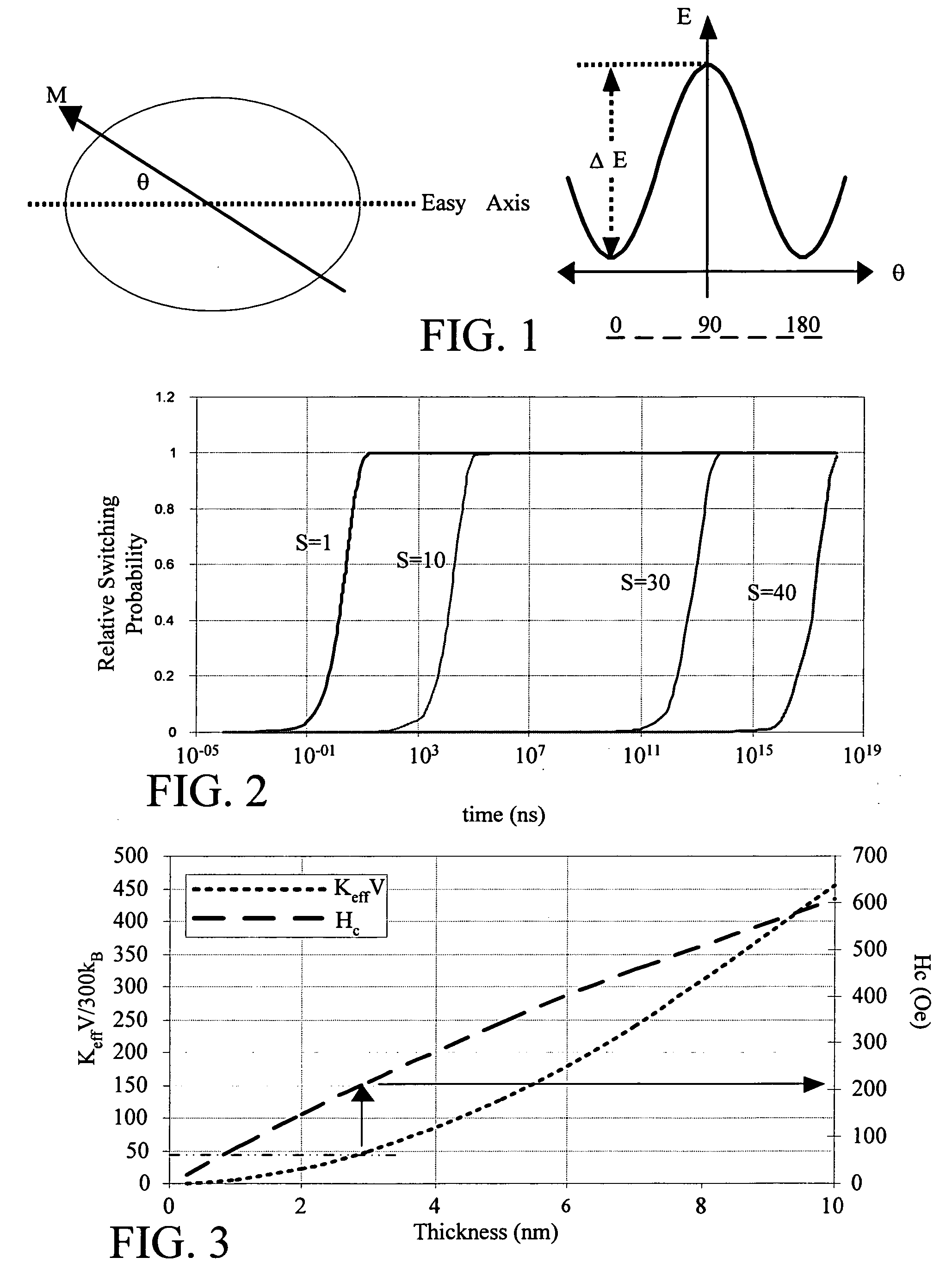
However, increasing Keff also increases the externally applied magnetic fields needed to be used for selecting the desired magnetic state in the memory element to represent current data therein, and so also the associated electrical currents by which the memory element is operated through generating such external fields, to impractical levels as indicated in FIG. 3.
This shows the difficulty in using only an externally applied magnetic field to provide such switching as generating a field in excess of 100 Oe is difficult in monolithic integrated circuit based magnetoresistive memory devices.

Method used


Image

  • Thermomagnetically assisted spin-momentum-transfer switching memory
  • Thermomagnetically assisted spin-momentum-transfer switching memory
  • Thermomagnetically assisted spin-momentum-transfer switching memory

Examples


Embodiment Construction

[0031] The electrical current needed for generating a resulting externally applied magnetic field to switch the magnetization direction in the free layer of a magnetoresistive memory device to a reverse position along the layer uniaxial anisotropy axis, or easy axis, can be too large to be practical as described above. This current magnitude can be reduced by supplementing the application of such switching current through additionally providing spin momentum transfer electrical currents in the device and resistive heating electrical currents in or adjacent to the device.

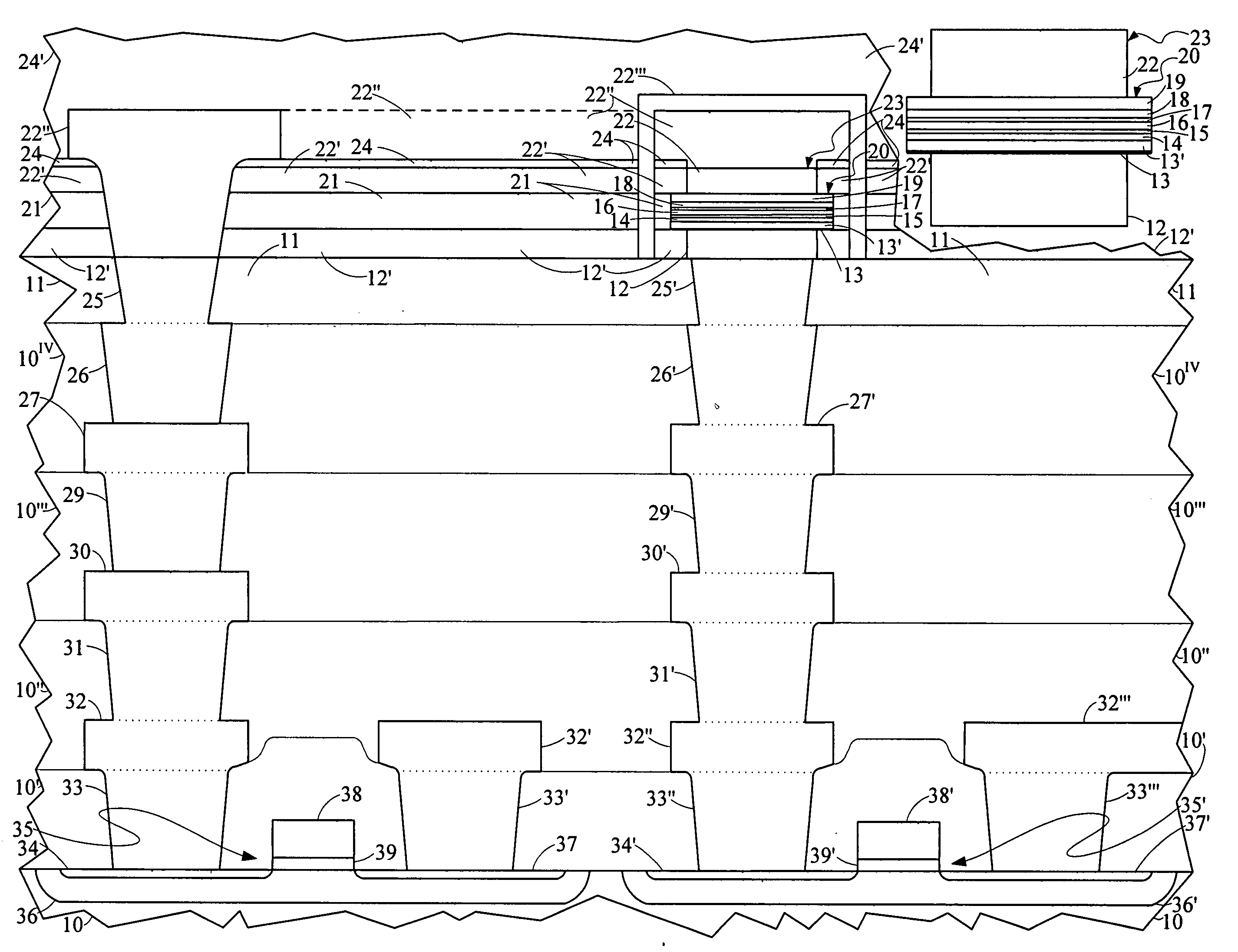
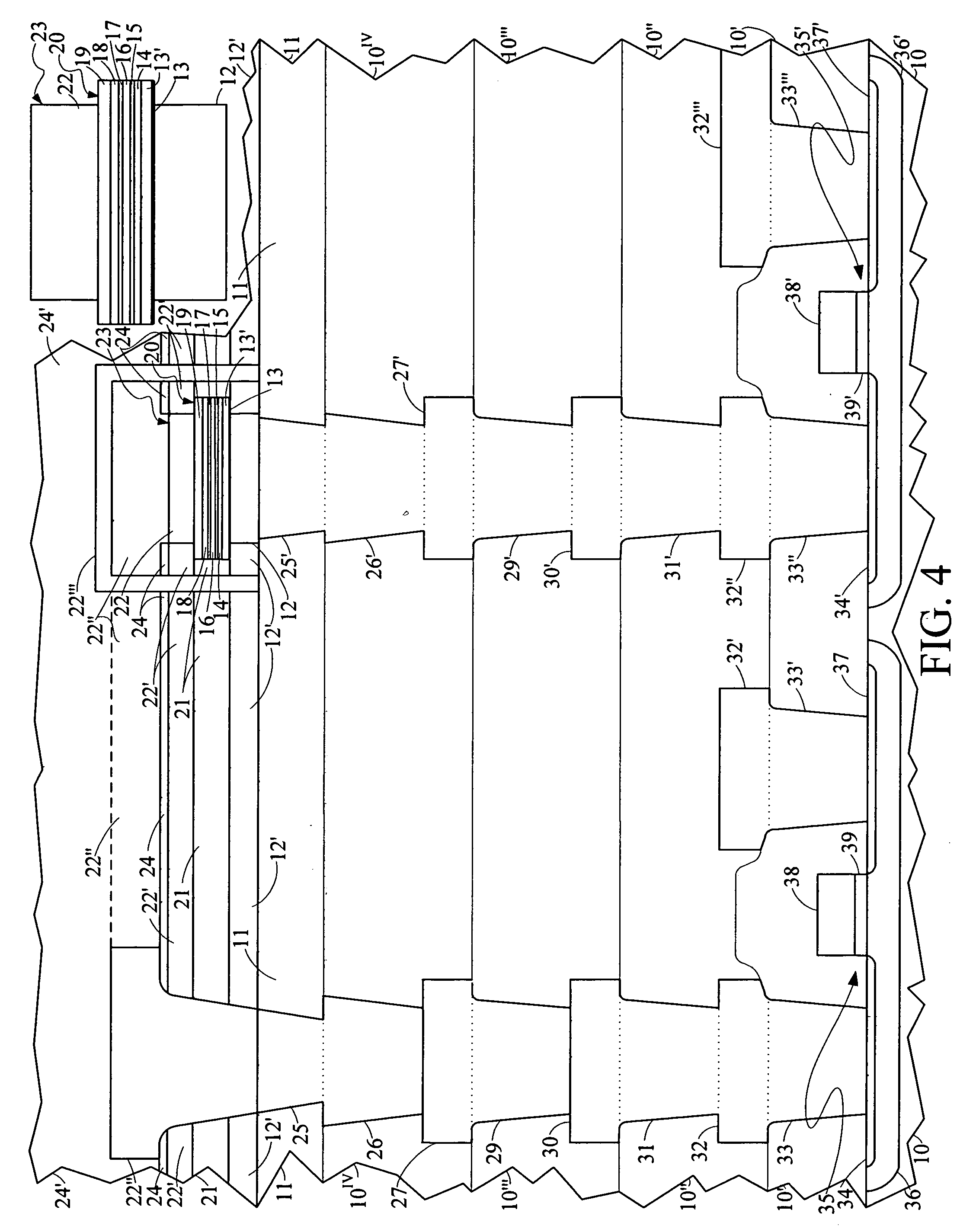
[0032] A monolithic integrated circuit structure example of such a magnetoresistive memory device arrangement suitable for this kind of operation is shown in a fragmentary view thereof in FIG. 4. There is shown a monolithic integrated circuit chip layer diagram of an external supplemented magnetic field switched memory element or cell magnetoresistive structure that is assisted in operation by supplemental spin mome...


PUM


Abstract

A ferromagnetic thin-film based digital memory having a substrate supporting bit structures that are electrically interconnected with information storage and retrieval circuitry and having first and second oppositely oriented relatively fixed magnetization layers and a ferromagnetic material film in which a characteristic magnetic property is substantially maintained below an associated critical temperature above which such magnetic property is not maintained. This ferromagnetic material film is separated from the first and second fixed magnetization films by corresponding layers of a nonmagnetic materials one being electrically insulative and that one remaining being electrically conductive. Each bit structure has an interconnection structure providing electrical contact thereto at a contact surface thereof substantially parallel to the intermediate layer positioned between the first contact surface and the substrate. A plurality of word line structures located across from a corresponding one of the bit structures on an opposite side. Electrical current selectively drawn through each of these bit structures and its interconnection structure can cause substantial heating of that bit structure to raise temperatures thereof while being above temperatures of at least an adjacent said bit structure because of sufficient thermal isolation.

Description

CROSS-REFERENCE TO RELATED APPLICATION [0001] This application claims the benefit of provisional Patent Application No. 60 / 617,954 filed Oct. 12, 2004 for “THERMALLY ASSISTED SPIN INJECTION SWITCHING MEMORY”.BACKGROUND OF THE INVENTION [0002] The present invention relates to ferromagnetic thin-film structures exhibiting relatively large response magnetoresistive characteristics and, more particularly, to such structures used for the storage and retrieval of digital data. [0003] Many kinds of electronic systems make use of magnetic devices including both digital systems, such as memories, and analog systems such as magnetic field sensors. Digital data memories are used extensively in digital systems of many kinds including computers and computer systems components, and digital signal processing systems. Such memories can be advantageously based on the storage of digital symbols as alternative states of magnetization in magnetic materials provided in each memory storage cell, the resu...

Claims


Application Information

Patent Timeline
Patent Type & Authority Applications(United States)
IPC IPC(8): G11C11/14
CPCG11C11/16H01L27/228H10B61/22
Inventor DEAK, JAMES G.
Owner NVE CORP
Learn More