Interdigitaded capacitors

a technology of interdigitated capacitors and capacitors, applied in the field of capacitors, can solve the problems of capacitor pair mismatch, capacitor precision matching,

Active Publication Date: 2006-03-16
BELL SEMICON LLC
View PDF7 Cites 15 Cited by
  • Summary
  • Abstract
  • Description
  • Claims
  • Application Information

AI Technical Summary

Benefits of technology

[0006] We have developed a new capacitor structure that employs interconnect metal in an interdigitated form, but provides additional simplification when capacitors are used in pairs. In addition, it significantly reduces structural variations between capacitors in a capacitor pair. According to the invention, paired capacitors are formed in an interdigitated configuration, in a manner that ensures that the plates of each pair occupy common area on the substrate. The interdigitated structure is laid-out such that structural anomalies due to process conditions are compensated in that a given anomaly affects both capacitors in the same way. Two of the capacitor plates, one plate for each of the matched pair of capacitors, are formed with electrically conductive comb structures, with the fingers of the combs interdigitated. The other plates for each of the capacitors are formed using one or more conductive runner structures interleaved between the interdigitated plates.

Problems solved by technology

While that approach is largely successful, precise matching of capacitors, even when formed side-by-side on a substrate wafer, may not result.
Capacitor pair mismatch commonly occurs due to localized thickness variations in the metal runners from one capacitor structure to another.

Method used


Image

  • Interdigitaded capacitors
  • Interdigitaded capacitors
  • Interdigitaded capacitors

Examples


Embodiment Construction

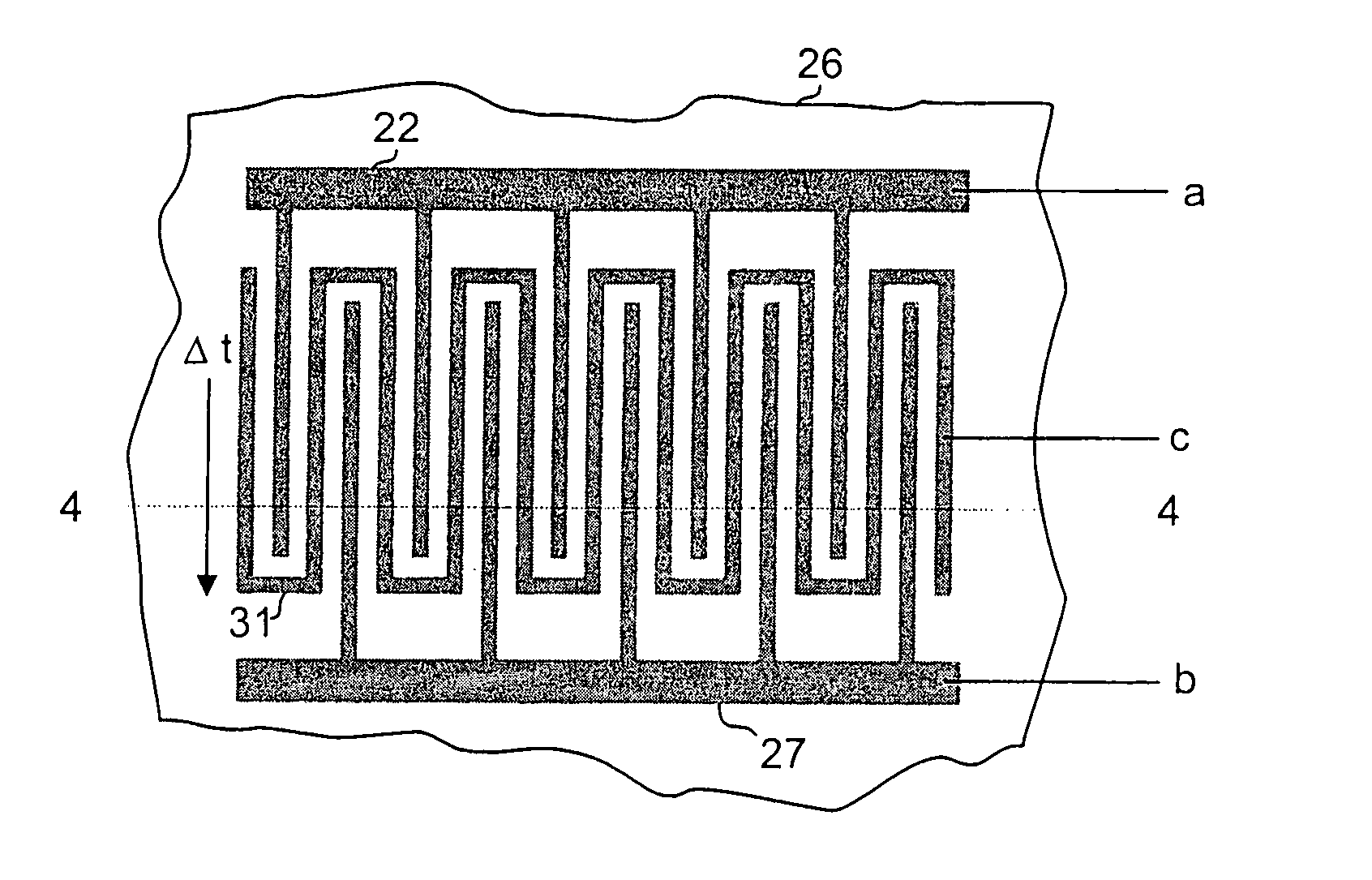
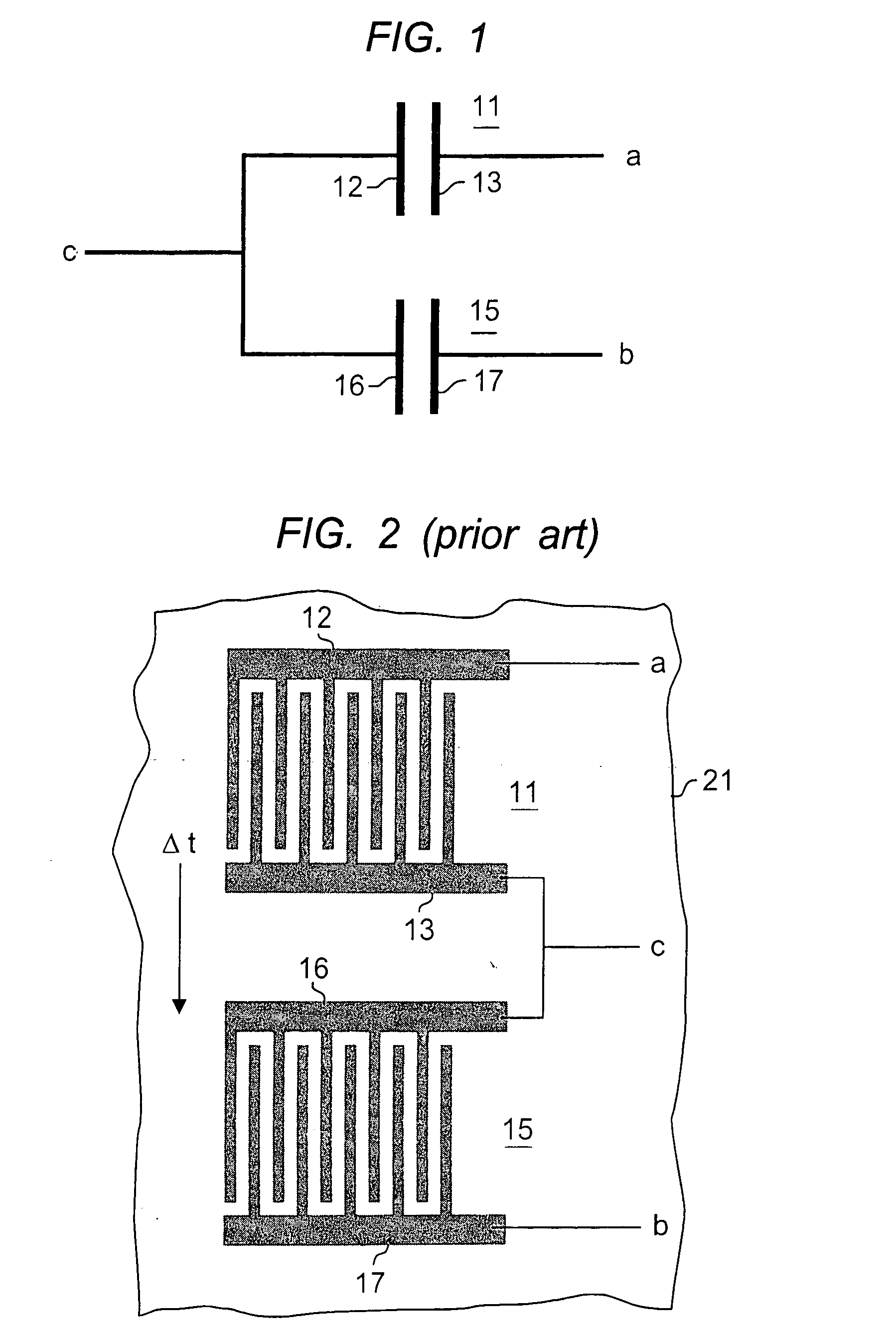
[0014]FIG. 1 shows one circuit embodiment of the invention that will be used for the detailed description. Capacitors 11 and 15 may be connected in the configuration shown, with I / O connections a, b, and c. Capacitor 11 is formed by plates 12 and 13, and capacitor 15 is formed by plates 16 and 17. This capacitor pair is shown implemented using an interdigitated interconnect structure in FIG. 2. Substrate 21 represents any known IC substrate including but not limited to silicon, gallium arsenide, indum phosphide or an IPD substrate such as ceramic. The substrate is shown cut-away indicating that this is a portion, typically a small portion, of a larger substrate or wafer.

[0015] Due to processing variables, it is not uncommon for the thickness of the blanket layer that is patterned to form the discrete interdigitated devices 11 and 15 in FIG. 2 to vary over the surface of the substrate. In IC device manufacture, the substrate is typically a silicon wafer with a plurality of identical...


PUM


Abstract

The specification describes matched capacitor pairs that employ interconnect metal in an interdigitated form, and are made with an area efficient configuration. In addition, structural variations between capacitors in the capacitor pair are minimized to provide optimum matching. According to the invention, the capacitor pairs are interdigitated in a manner that ensures that the plates of each pair occupy common area on the substrate. Structural anomalies due to process conditions are compensated in that a given anomaly affects both capacitors in the same way. Two of the capacitor plates, one in each pair, are formed of comb structures, with the fingers of the combs interdigitated. The other plates are formed using one or more plates interleaved between the interdigitated plates.

Description

RELATED APLICATIONS [0001] This application is a division of application Ser. No. 10 / 886,763 filed Jul. 8, 2004FIELD OF THE INVENTION [0002] This invention relates to capacitors for integrated circuits. BACKGROUND OF THE INVENTION [0003] A simple and cost-effective way of forming capacitors for integrated circuits is to use side-by-side runners of interconnect metal. To enhance capacitor area the runners may be interdigitated. See U.S. Pat. No. 6,383,858, issued May 7, 2002, and incorporated herein by reference. Since the capacitor dielectric may be formed by the interlevel dielectric of the integrated circuit (IC) these passive devices can be formed with no additional IC processing steps. Capacitance may be further increased by stacking interdigitated structures in a multi-level configuration. (See the patent referenced above). [0004] Capacitors of this type may be integrated with active devices in a conventional integrated circuit, or may comprise portions of integrated passive de...

Claims


Application Information

Patent Timeline
Patent Type & Authority Applications(United States)
IPC IPC(8): H01L29/00
CPCH01L23/5223H01L28/82H01L28/40H01L27/0805H01L2924/0002
Inventor HARRIS, EDWARD B.HE, CANZHONGLEUNG, CHE CHOIMCNEILL, BRUCE W.
Owner BELL SEMICON LLC
Why Eureka
Try Eureka