Method for planarizing polysilicon

Inactive Publication Date: 2006-03-02
IND TECH RES INST
View PDF5 Cites 20 Cited by
  • Summary
  • Abstract
  • Description
  • Claims
  • Application Information

AI Technical Summary

Benefits of technology

[0009] To overcome the above problems, an object of the invention is to provide a method for planarizing polysilicon that can be used with large-size polysilicon substrates. The method includes etching the polysilicon to change its surface morphology by the removal of native oxide, weak bonded silicon, and impurities in the polysilicon to initially lower the surface roughness. The etching process is followed by a laser annealing process to partially melt the polysilicon so that the surface of polysilicon is reconstructed to form a smooth surface. By adjusting etching and laser annealing, a relatively smooth polysilicon surface can be obtained.
[0010] In order to achieve the above objects, there is provided a method for planarizing polysilicon, including providing a substrate formed with polysilicon on the surface, changing surface morphology of the polysilicon by etching to initially reduce surface roughness, and laser annealing the polysilicon to partially melt and thereby planarize the surface thereof.
[0013] According to the method of the present invention, after the polysilicon surface is modified by etching, laser annealing is then carried out to obtain a smooth surface. The method of the present invention advantageously achieves reduced surface roughness and is suitable for use in large-size polysilicon substrates.

Problems solved by technology

A problem with current polysilicon TFT processes is surface roughness, which becomes more serious as grain size of polysilicon continues to increase.
The surface roughness issue is disadvantageous for the electrical properties of the devices in, for example, breakdown electrical field, leakage current, sub-threshold swing, threshold voltage and mobility of electron / hole.
Undesirable surface roughness of polysilicon may directly impact product quality and yield.
Reliability of devices is adversely affected, and may even become worse in the case of thin gate insulator devices.
Furthermore, during photolithography processes, undesirable surface roughness of polysilicon may cause disorder scattering, resulting in inaccuracy of pattern size definition.
Current planarization using CMP, however, is not suitable because no CMP equipment is designed for use with such large-size polysilicon substrates.
CMP may be no longer applicable in the future for mass production of large-size polysilicon substrates.
Furthermore, the surface roughness of polysilicon after CMP processing may still be as high as 30 or 40 angstroms, which is not acceptable for advanced TFT devices of reduced dimensions.

Method used


Image

  • Method for planarizing polysilicon
  • Method for planarizing polysilicon
  • Method for planarizing polysilicon

Examples


Embodiment Construction

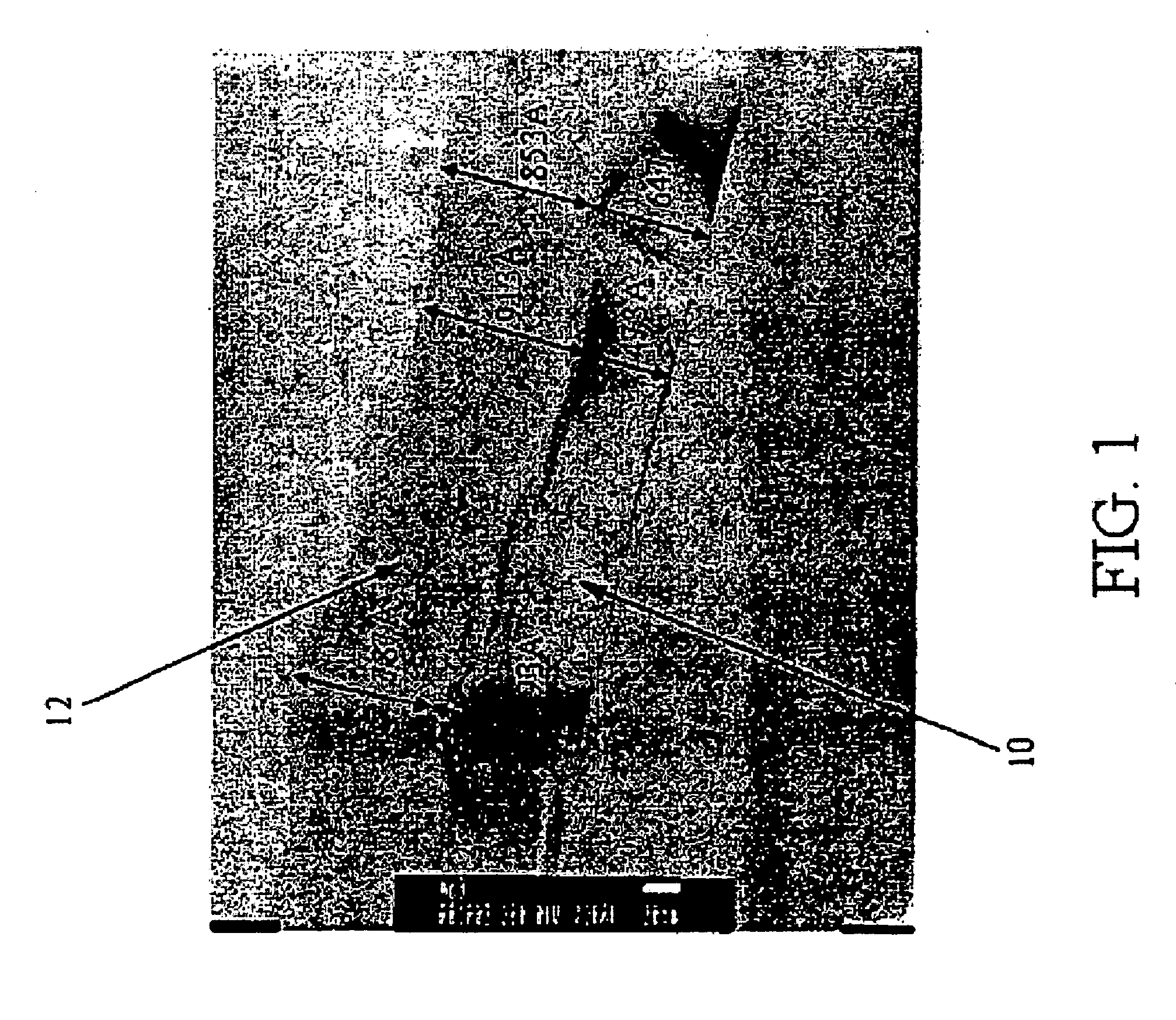
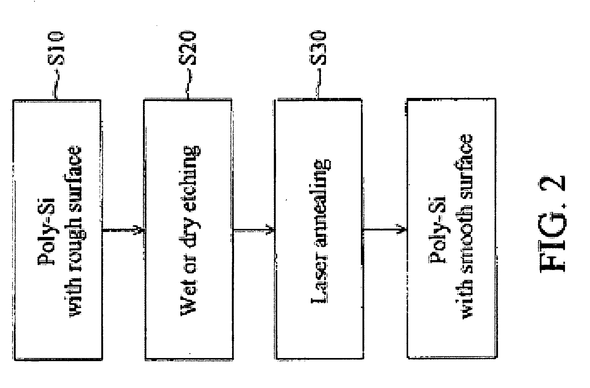
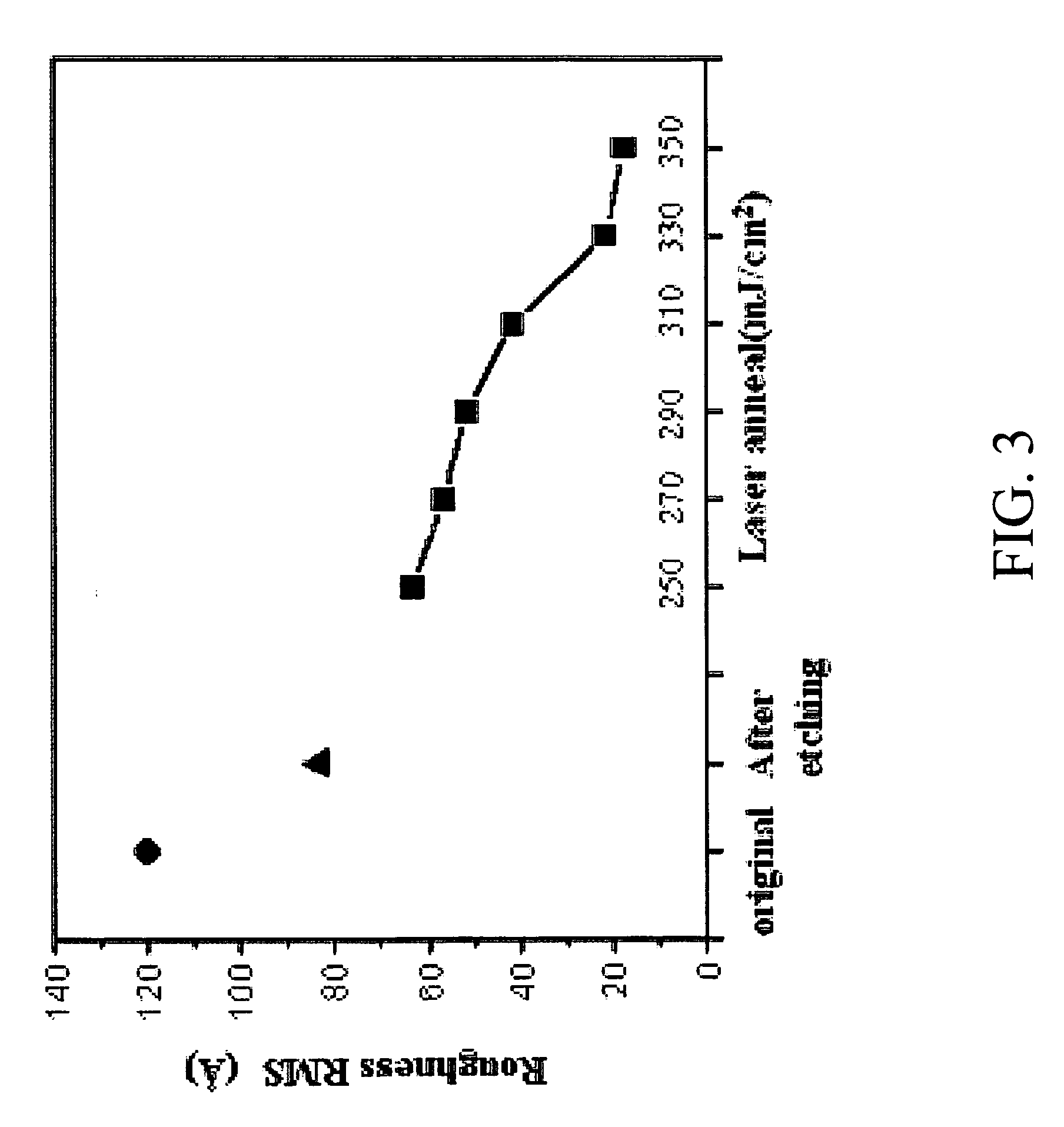
[0033]FIG. 2 illustrates a process flow of a method for planarizing polysilicon in accordance with one embodiment of the present invention. Referring to FIG. 2, a substrate formed with polysilicon on a surface is provided at step S10. Formation of the polysilicon is not restricted to a particular method, and may be attained by, for example, laser crystallization or chemical vapor deposition. Next, at step S20, an etching process is carried out to change the surface structure of the polysilicon. In one embodiment, buffered oxide etchant (“BOE”) is used as an etching solution. During the etching process, native oxide, weak bonded silicon and impurities in the polysilicon surface are removed. Components of the BOE solution are HF, NH4F and H2O. A preferable ratio of the BOE to water is 1:300˜1:0. In another embodiment, diluted hydrogen fluoride (“DHF”) is used as an etching solution. The preferable ratio of hydrogen fluoride to water is 1:600˜1:1. Preferable time for wet etching is les...


PUM

PropertyMeasurementUnit
Fractionaaaaaaaaaa
Densityaaaaaaaaaa
Ratioaaaaaaaaaa

Abstract

A method for planarizing polysilicon comprises providing a substrate, forming a dielectric layer on the substrate, forming an amorphous silicon film on the dielectric layer, etching the amorphous silicon film to remove native oxide formed on a surface of the amorphous silicon film, exposing the surface of the amorphous silicon film to a first radiation source to polycrystallize the amorphous silicon film into a polysilicon film, etching the polysilicon film to remove weak bonded silicon formed on a surface of the polysilicon film, and exposing the surface of the polysilicon film to a second radiation source to reflow the polysilicon film.

Description

CROSS-REFERENCE TO RELATED APPLICATIONS [0001] This application is a continuation-in-part of U.S. patent application Ser. No. 10 / 358,184, filed Feb. 5, 2003, which is herein incorporated by reference in its entirety.BACKGROUND OF THE INVENTION [0002] 1. Technical Field of the Invention [0003] The present invention generally relates to a method for planarizing polysilicon and, more particularly, to a method which includes providing a substrate with polysilicon on the surface, etching the surface of the polysilicon to initially reduce surface roughness, and laser annealing the polysilicon to partially melt the polysilicon to planarize the surface thereof. [0004] 2. Description of the Related Art [0005] Polysilicon thin film transistors (“TFTs”) have been widely used in various fields, such as active matrix liquid crystal displays (“LCDs”), active matrix organic light-emitting displays, static random access memory (“SRAM”) devices, projectors and contact type image sensors. A problem w...

Claims


Application Information

Patent Timeline
IPC IPC(8): C03C15/00
CPCC03C15/00C03C15/02C03C23/0025H01L29/78606H01L21/32115H01L29/6675H01L21/2026H01L21/02686H01L21/02691H01L21/02488H01L21/02422H01L21/02592H01L21/02532H01L21/02502H01L21/02595H01L21/02675
Inventor CHEN, YU-CHENGLIN, JIA-XINGCHEN, CHI-LIN
Owner IND TECH RES INST
Why Eureka
Try Eureka