
Method of manufacturing laminate for flexible printed circuit board

a printing circuit board and flexible technology, applied in the direction of resistive material coating, chemical vapor deposition coating, metallic material coating process, etc., can solve the problems of unsuitable use in high density circuit patterns, remarkably weak adhesive strength between metal foils and polyimide films, and insufficient adhesive strength and heat resistance. to achieve the effect of high adhesive strength

Inactive Publication Date: 2006-02-02
TORAY SAEHAN
View PDF15 Cites 11 Cited by
  • Summary
  • Abstract
  • Description
  • Claims
  • Application Information

AI Technical Summary

Benefits of technology

[0015] Accordingly, the present invention has been made keeping in mind the above problems occurring in the prior art, and an object of the present invention is to provide a method of manufacturing a laminate for an FPCB, which comprises surface treating a base film to have higher adhesive strength between the base film and a metal foil, heat resistance and dimensional stability.
[0016] Another object of the present invention is to provide a method of manufacturing a laminate for an FPCB, which can increase the treatment rate compared to a conventional surface treatment using plasma, to realize high productivity.

Problems solved by technology

However, since the three-layered substrate may cause the above problems due to the use of the adhesive, it is unsuitable for use in a high density circuit pattern.
However, the adhesive strength between the metal foil and the polyimide film is remarkably weakened.
Although the plasma treatment is conducted for two purposes, that is, washing and good adhesion, the adhesive strength and heat resistance are not increased as high as desired.

Method used


Image

  • Method of manufacturing laminate for flexible printed circuit board
  • Method of manufacturing laminate for flexible printed circuit board
  • Method of manufacturing laminate for flexible printed circuit board

Examples


Embodiment Construction

[0029] Hereinafter, a detailed description will be given of the present invention, with reference to the appended drawings.

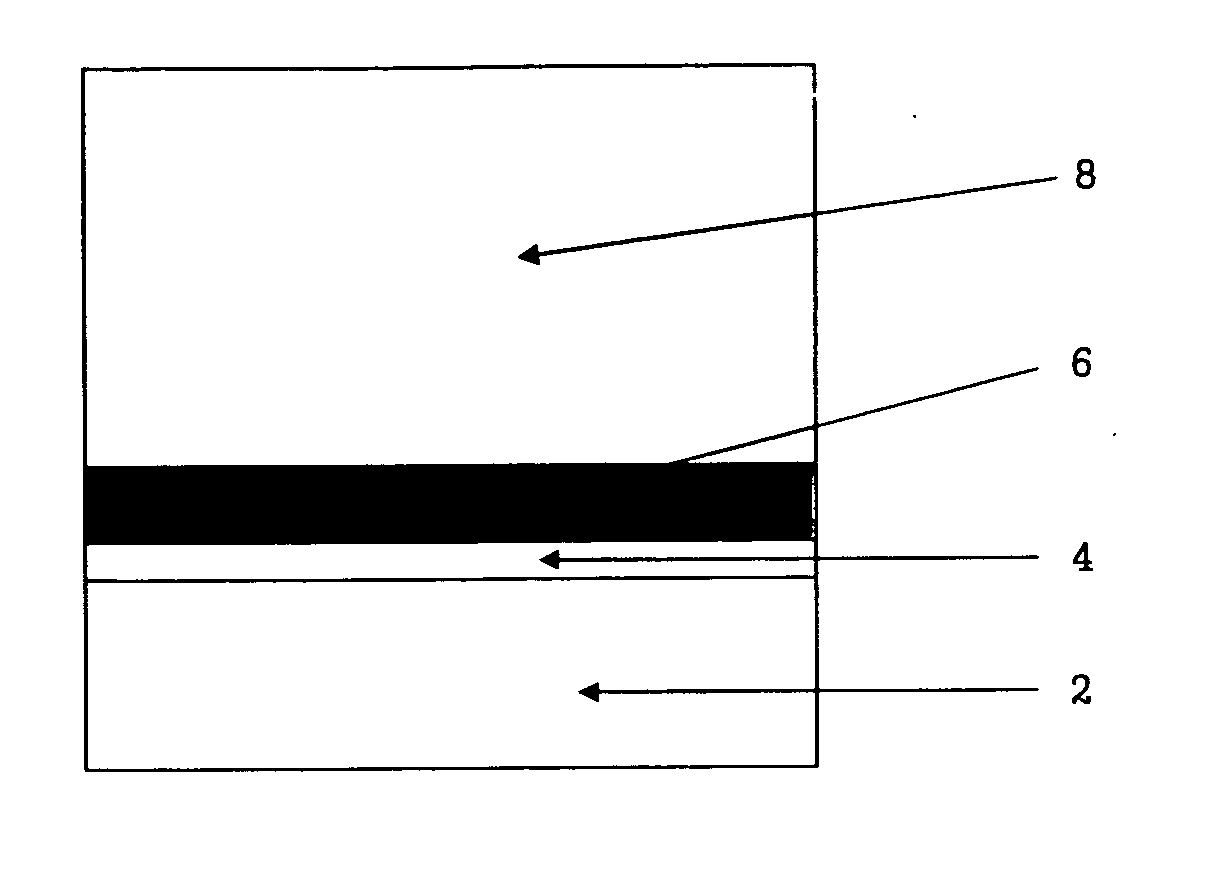
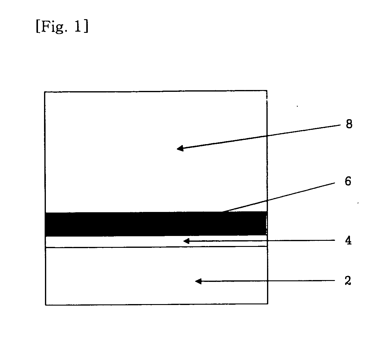
[0030]FIG. 1 is a sectional view showing a two-layered substrate for an FPCB, according to the present invention.

[0031] As shown in FIG. 1, the two-layered substrate for an FPCB comprises a lower base film 2, a 5-20 nm thick tie layer 4 laminated on the base film 2, a metal conductive layer 6 laminated on the tie layer 4, and a metal plated layer 8 formed on the metal conductive layer 6 through plating of the metal conductive layer 6 using a photoresist composition.

[0032] The tie layer 4 functions to prevent the diffusion of a metal to be laminated and increase the adhesive strength, and is typically formed of Cr, Ni—Cr alloy, monel (Ni—Cu alloy), etc. In the present invention, a Cu—Ta—Zn alloy or a Cu—V—Zn alloy (hereinafter, referred to as ‘CAT alloy’) has first been used for the tie layer. When using a Cu—Ta—Zn alloy at a % ratio of 95:1:4 or a Cu—V—Zn all...


PUM

PropertyMeasurementUnit
Fractionaaaaaaaaaa
Fractionaaaaaaaaaa
Dimensional stabilityaaaaaaaaaa

Abstract

Disclosed herein is a method of manufacturing a laminate for a flexible printed circuit board, in which a base film is surface treated by radiating ion beams using a gas mixture comprising oxygen and argon. According to the method of the current invention, a laminate for a flexible printed circuit board, having high adhesive strength, heat resistance, dimensional stability, and productivity, can be manufactured.

Description

BACKGROUND OF THE INVENTION [0001] 1. Field of the Invention [0002] The present invention relates, generally, to a method of manufacturing a laminate including a base film and a metal foil for use in fabrication of a flexible printed circuit board (FPCB), and, more particularly, to a method of manufacturing a laminate for an FPCB, which comprises surface treating a base film to have excellent adhesive strength, heat resistance and dimensional stability. [0003] 2. Description of the Related Art [0004] According to a recent tendency toward light weight, miniaturization, and high functionality of electronic products, PCBs have been increasingly used. Of the PCBs, in particular, an FPCB is advantageous because a circuit can be effectively formed even in a narrow space due to the use of a flexible and thin material, and the demand therefor is rapidly increasing. [0005] In general, the FPCB includes a base film made of polyimide, polyester, or polyparavinyl acid, and a conductive metal fo...

Claims


Application Information

Patent Timeline
IPC IPC(8): B05D5/12
CPCC08J7/123C08J2379/08C23C14/022C23C14/028H05K2203/095H05K3/381H05K3/388H05K2203/092H05K1/0393H05K3/38
Inventor CHO, JEONGLEE, YOUNG KWANKIM, YOUNG SEOP
Owner TORAY SAEHAN
Learn More